Stackup
- Coating: Conformal coating material applied to protect the top and bottom signal layers.
- Dielectric: Dielectric layer between two conductor layers. Multiple dielectric layers can be placed next to each other
- Signal: Etched signal layer. Core signal layer when microvias are used.
- Micro Signal: For boards using microvias. Micro signal layers are made on both sides of board. Microvias are used for connecting micro signal layers or connecting a micro signal layer and the first core layer.
- Power: Power plane layer.
- Ground: Ground plane layer.
- Floating: Floating conductor plane layer.
- Often the top and bottom widths of etched conductor trace cross-section are different, resulting in a trapezoidal cross-section shape.
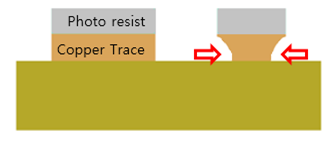
You can define PCB trace etching effect. The value of etching difference can be typed
in after double clicking the area of numbers assigned and the etching surface
direction can be defined by clicking ![]() .
.
PollEx PCB provides default layer stack set and you can add
or edit layer stack by clicking Import or
Export. The default layer stack file path is:
Installed directory/Data/Layer.
You can add, remove, or insert each layer by clicking Add, Remove, or Insert. By selecting this menu, the Add dialog opens. Use the Add dialog to material characteristics.
You can export stack-up information into Excel format file.