This section contains the user guides for the following tools: Block JIG Generator, Compare GDSII, Gerber to PCB,
Make Board Paneling, Metal Mask Manager, Mounting Data Extractor, Mounting Emulator, Router-Machine JIG Generator,
Solder Quantity Calculator, Soldering Pallet, Test Point Location Generator, and Underfill.
This section contains the user guides for the following tools: BOM, CAM, Component Arrangement Plan, CP, Golden Sample,
Logic, PCB, Redmark+, and Worksheet Planner.
Use various modelers and editors in this menu to make simulation model libraries, general information properites,
and configuration tables for logic symbols and footprints automatic generation.
Define the general information properties of the components such as product families, usage keys, user defined part
classifications, package types and manufacturer lists.
Create and edit the configuration table for automatic generation of logic symbols and footprints, and make the functional
logic symbols for automatic logic symbol generation.
Define the files and folders such as part library folder, general information files and configuration table files.
You also can define the initial view configurations and ECAD interface settings.
Use various modelers and editors in this menu to make simulation model libraries, general information properites,
and configuration tables for logic symbols and footprints automatic generation.
Create and edit the configuration table for automatic generation of logic symbols and footprints, and make the functional
logic symbols for automatic logic symbol generation.
Definition if the Pin Pad Size Input Type is Margin from Drill Hole.
Top Layer: Define the pad shape and size for the top layer.
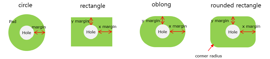
Connect Pad: Define the connected pad shape and size of the top
layer.
Pad Shape: Define connected pad shape from Circle, Rectangle,
Oblong, or Rounded Rectangle.
Define size: Circle (margin from drill hole), Rectangle/Oblong
(X/Y margin from drill hole), and Rounded Rectangle (X/Y margin
from drill hole and Rounded corner radius) respectively.
Figure 2.
Solder Resist: Define the solder resist pad size using margin from the
pad.
Figure 3.
Unconnected pad: Define the unconnected pad shape and size.
If unconnected pad is needed, select the check box.
Define the pad shape and size.
Thremal pad: Define the thermal pad shape and size.
If thermal pad is needed, select the check box.
Thermal pad shape: Select the thermal pad shape.
Circle and Square shapes available.
Number of spokes: Select the counts of spokes (2 or 4).
Spoke width: Define the width of the spoke.
Anti-Pad Margin from Drill Hole: Define the pad margin from drill
hole.
Figure 4.
Bottom layer: Define the pad shape and size for the bottom layer.
The definition method is the same as the top layer.
Inner signal layer: Define the pad shape and size for the inner signal layer.
The definition method is the same as the top layer, with the additional option
for solder resist definition.
Inner plane layer: Define the pad shape and size for the inner plane layer.
The definition method is the same as the top layer, with the additional option
for solder resist definition.