PCB Layer Stack-up
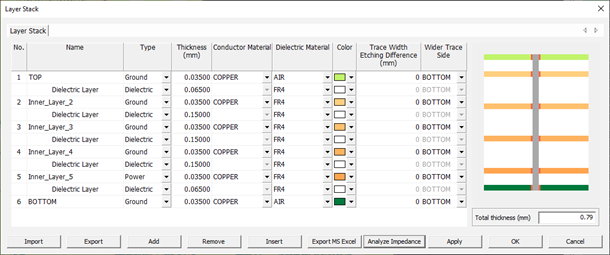
The Properties > Layer Stack menu shows the physical stack-up information of PCB which are needed for thermal, signal integrity, and power integrity analyses. The layer stacking order and the thicknesses and material properties of the metallic and dielectric layers are required properties for such analyses.
New layer thickness values can be entered after double-clicking the currently listed value. Other parameters can be defined by clicking and selecting one of the drop-down values. Type of a power plane layer should be defined as Power while Type of a ground plane layer should be defined as Ground, as shown below.
You can define the etching effect of PCB traces. The value of etched trace top and
bottom width difference can be entered after double-clicking the value field, and
the wider trace side (top or bottom) can be defined by clicking ![]() .
.
PollEx PCB provides a default layer stack set, and you can bring in a new layer stack set or save the current layer stack set in a layer stack file by clicking Import or Export, respectively. The default layer stack file is in the folder of Installed directory/Polliwog/Data/Layer. You can add, remove, or insert a layer by clicking Add, Remove, or Insert, respectively. Upon clicking Add or Insert, the Add dialog opens. You can define the layer properties.
