PollEx Overview
Altair PollEx is a PCB-level Electronic Design Automation (EDA) software suite covering design review, analysis and manufacturing.
Altair PollEx significantly reduces development cycles while providing a common communication application between schematic engineers, PCB designers, CAE analysts, and manufacturing engineers.
PollEx can import designs from different major ECAD vendors, such as Cadence, Mentor Graphics, Zuken and Altium, as well as industrial neutral formats like ODB++ and IPC2581. Using the imported PCB design, PollEx supports verification of design for manufacturability (DFM), design for assembly (DFA), and design for electrical engineering (DFE), along with analyses (SI, PI, and Thermal).
PollEx PCB Modeler supports design review, query, search, measure, net 3D, net topology, data extraction and the possibility to save and securely share specific areas of the design. In addition, it supports schematic and Gerber design reviews. Another powerful function is the automatic comparison between PCB designs, schematics and BOM data.
PollEx PCB Verification checks the quality of designs in terms of manufacturing, assembly and electrical engineering. It provides intuitive rule definitions via input dialogs, advanced results viewing and easy documentation features.
PollEx PCB Solvers provide signal integrity and board level thermal analysis. For signal integrity, PollEx is based on 2D and 3D electromagnetic field solvers providing different types of analysis, including transmission line, eye diagram and crosstalk analysis, besides network RLGC parameters extraction. For thermal analysis, based on FEM, PollEx calculates heat dissipation from components on boards. All analyses are supported by a built-in material library, with parts’ properties obtained from Unified Part Libraries (UPFs).
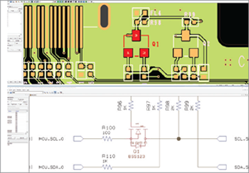
Easily and automatically review and compare PCB designs using PollEx PCB Modeler.
Detect 900+ different design defects in early design stages with PollEx PCB Verification.
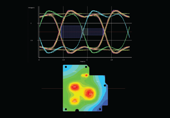
Analysis of signal integrity and thermal problems via PollEx Solvers.
Product Highlights
- Easy-to-use collaborative application to quickly visualize and review PCB designs.
- Unsurpassed connectivity to major ECAD systems.
- Powerful rule-based checking tools (DFM, DFA and DFE) to detect faults early in design.
- Easy solution for SI and thermal analysis of PCBs using the integrated parts and material libraries.
Benefits of PollEx
- Savings in ECAD Licenses
- Maximize work efficiency through improved communication among engineers from different disciplines making the same product. PollEx PCB Modeler aids better quality products by sharing schematics, PCBs and Gerber files without the need for expensive ECAD licenses.
- Detect Design Faults in Early Design Stages
- Various problems occurring post-design are difficult and costly to solve. PollEx PCB Verification enables significant cost-savings by detecting manufacturing, assembly and electrical defects and faults early in the designs. Validating designs based on rules from accumulated customers’ know-how consistently maintains the highest design quality.
- Easy, Fast, and Accurate Analysis
- PollEx PCB Solvers resolve electrical and thermal problems at early design stages. Using an easy link to the components’ library, a board setup based on a built-in materials library and combining 2D and 3D parasitic model extraction analysis, the solvers provide fast and accurate results. In addition, PollEx DFE+ offers a new unique solution by combining analysis with verification, which enables engineers to incorporate know-how generated in the current analysis into the next PCB design.
PollEx Capabilities
Altair PollEx contains the following capabilities.
ECAD Design Review
- Schematic design review from all major EDA vendors
- Gerber (274D, 274X) data review
- PCB design review from all major EDA ECAD vendors
- Comparison between PCB-to-PCB and schematic-to-schematic designs
- Comparison among PCB, schematic and BOM
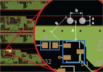
- Artwork/physical/composition layer view, query, search, and measure for PCB objects
- Part, net, pad stack and via library
- Save arbitrary design shapes under a different name with a reduced file size, with a password
- Red-Mark (+) feature for comments
- Net 2D/3D display, net topology display and automatic composite net generation
Verification: DFM, DFE, and DFA
- Checking items for DFM (500+), DFE (300+), DFA (50+) and DFE+ (50+)
- DFM covers the manufacturing areas of board, component, drill, FPCB, package, pad, pattern, placement, and tooling.
- DFE covers the electrical areas of high-speed signals, differential pairs, common nets, power, filters, components, and boards.
- DFA covers the manufacturing assembly areas of collision, lead, placement, component and board.
- DFE+ provides verification linked to solvers for signal integrity and thermal analysis.
- Export customized and formatted Excel reports of verification results.
Analysis: Signal Integrity, Power Integrity, and Thermal
- Built-in material library
- Signal integrity
- Transmission line analysis: TML analysis and trace optimization
- Network analysis: Waveform analysis, eye diagram analysis, and network parameters (RLCG)
- Crosstalk analysis
- Net topology analysis, including topology editing function
- Radiated Emission: Analyze current of trace in Time-Dimain and Frequency-Domain. The resulting .rei file is used as an EMI noise source in an EM solver such as Feko
- Power Integrity
- Handles multi-layer and multi-reference power-ground planes of arbitrary-shape
- Modular, comprehensive finite element modeling
- Models for skin effect loss and board/package edge radiated emissions
- 3D model of via discontinuity
- Model of split plane discontinuity effects to allow for handling multiple reference planes
- Outputs multi-port impedance matrix network for PDN and IR-Drop
- Thermal
- Built-in package-dependent thermal resistance values for components
- 3D finite element steady-state analysis results for thermal board contour, board top/bottom, and component junction temperature
- Perform PCB level thermal analysis including Jouleheat of trace.