Open the
PollEx_PCB_Sample_r<revision_number>.pdbb
file from
C:\ProgramData\altair\PollEx\<version>\Examples\PollEx_PCB_Sample_r<revision_number>.pdbb.
Click File > Save As Project.
The Save As Project dialog displays.
Enter a new project name and select the project folder to put in the design
folder.
Click OK.
The project directory is created under the design folder, and
PollEx_PCB_Sample_r<revision_number>.pdbb
and related files are copied into the project directory. The Part directory is
created.
Click File > Exit to close this design.
Add New Dielectric Material
In this step, you will add a new dielectric material FR4.- and PSR3.0.
Click File > Open.
Open the Project
Directory/PollEx_PCB_Sample_r<revision_number>.pdbb
file.
You should open the .pdbb file in the project
directory.
Click Properties > Material Library.
The Materials dialog opens.
Add FR4.0.
From the Materials dialog, click Add
Dielectric.
The Edit dialog opens.Figure 1.
For Material name, enter FR4.0.
For X, Y, and Z, enter 0.35.
For Dielectric Constant, enter 4.0.
For Loss Tangent, enter 0.02.
Figure 2.
Click OK to close the
Edit dialog.
Add PSR3.0 for solder resist layer.
From the Materials dialog, click Add
Dielectric.
The Edit dialog opens.
For Material name, enter PSR3.0.
For X, Y, and Z, enter 0.35.
For Dielectric Constant, enter 3.0.
For Loss Tangent, enter 0.02.
Figure 3.
Click OK to close the
Edit dialog.
The FR4.0 and PSR3.0 materials are registered as new
materials.Figure 4.
Click OK to close the
Materials dialog.
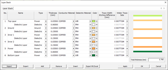
Build PCB Stack
Click Properties > Layer Stack.
You can set the Layer Stack by referring to the PCB_stackup_New_Sample.xlsx
file.
The PCB_stackup_New_Sample.xlsx file is located at
C:\ProgramData\altair\PollEx\<version>\Examples\Slver\PI\Stackup.
The Layer Stack dialog opens.
Enter Thickness and Dielectric Material fields by referring to the values in
the PCB_stackup_New_Sample.xlsx file.
Change the layer Type.
Figure 5.
Execute the Export menu to save current layer stack information.
The Explorer dialog displays.
Enter StandardStackup_PI.udls as the new
stack-up file name.
Click OK to close the
Explorer dialog.
Tip: You can import this layer stack
information again by executing the Import menu.
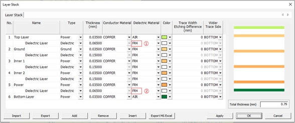
Change Dielectric Constant.
Figure 6.
Click and select
FR4.0.
The dielectric constant for TOP layer changes from 4.5 to
4.0.
Click and select
FR4.0.
The dielectric constant for Bottom layer changes from 4.5 to
4.0. 5.
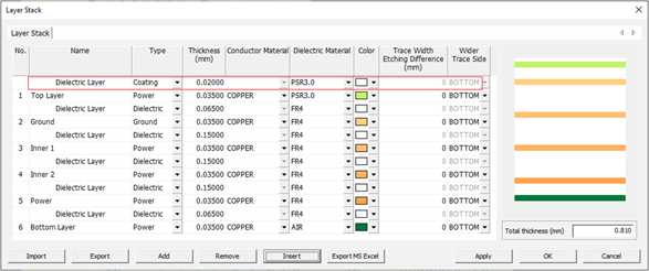
Add Solder resist layer to the Top layer and Bottom Layer.
Select Top layer and click Insert.
The Add dialog displays.
Select Coating as the Type.
Select PSR3.0 for the Dielectric material.
Enter 0.02 for the Thickness.
Figure 7.
Click OK to close the
dialog.
The new Solder Resist layer is inserted at the top.Figure 8.
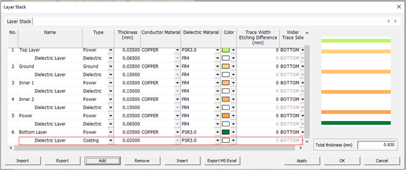
Select Bottom layer and click
Add.
The Add dialog opens.
Select Coating for the Type.
Select PSR3.0 for the Dielectric material.
Enter 0.02 for Thickness.
Figure 9.
Click OK to close the
dialog.
The new Solder Resist layer is inserted at the bottom.Figure 10.
Click Export to save this stack-up.
The Explorer dialog opens.
Enter StandardStackup_PSR as the new stack-up
file name.
Click Import to load pre-saved layer stackup
(StandardStackup_PI.udls).
The Explorer dialog opens.
Find the directory path for your stack-up files
(StandardStackup_PI.udls) in the navigation
tree.
All stackup files for tutorial are located at
C:\ProgramData\altair\PollEx\<version>\Examples\Slver\PI\Stackup.
Select StandardStackup_PI.udls and click
Open to open this stack-up.
Figure 11.
Click OK to close the
Layer Stack dialog.
Assign IBIS Model
In this step, you will assign an IBIS model to a DDR3 memory device.
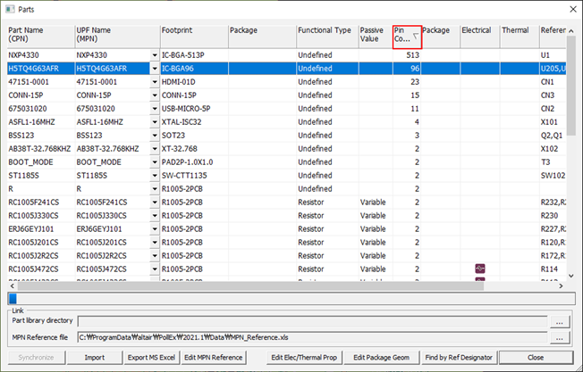
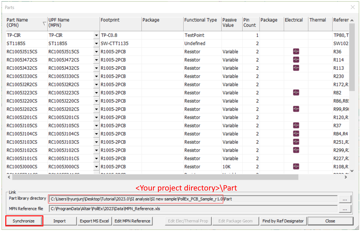
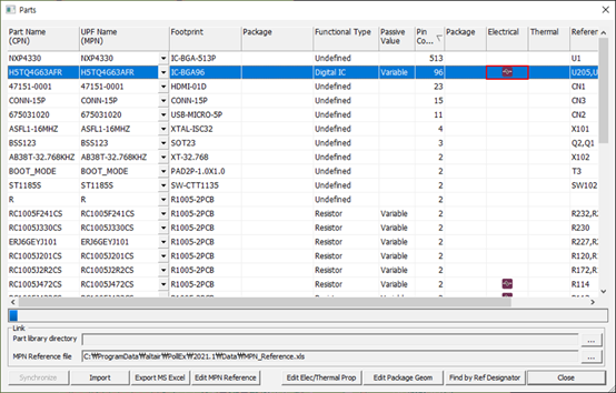
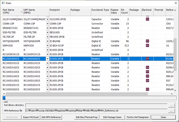
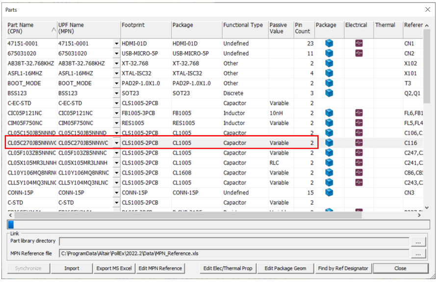
Click Properties > Parts.
The passive component RLC values are automatically extracted from PDBB data,
if the value property was correctly assigned in the PDBB database.Figure 12.
The Parts dialog opens.
First, before assign IBIS model, Part library directory should be
assigned on your project directory's parts folder. The project directory means
that it was specified through the 'Save as project' at the beginning of the
tutorial.
Part library directory path : <your project
directory>\Part
Click Synchronize.
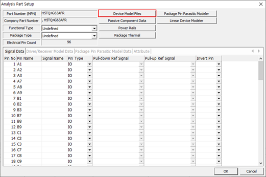
Double-click H5TQ4G63AFR.
The Electrical & Thermal Properties dialog
displays.
Assign Simulation Model.
Click Device Model Files.
Figure 13.
The Device Model Files dialog
opens.
Click Add in the Device Model
Files dialog.
The Model File dialog opens.
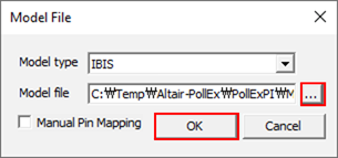
Click to search and select the IBIS file
(C:\ProgramData\altair\PollEx\<version>\Examples\Solver\PI\Simulation_Model\Memory.ibs)
for DDR3 Memory device and click Open.
Figure 14.
Click OK to close the
Model Files dialog.
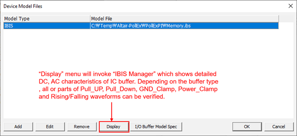
The full location of the IBIS model file assigned to the DDR3 Memory
device is shown in the Device Model Files dialog.
After selecting the added IBIS file, the Display menu allows you to
investigate the detailed electrical properties of the Input/output
buffer models included in the IBIS file. Input buffer models only
contain Power_Clamp and Ground_Clamp characteristics. The DC (I-V)
properties of Pull_Up and Pull_Down transistors and AC properties given
in Rising/Falling waveforms are just related to the Output and IO buffer
models. The DC, AC information for Input buffer models cannot be
found.
The Device Model Files dialog
opens.
Click Display to open the IBIS
Manager dialog.
Figure 15.
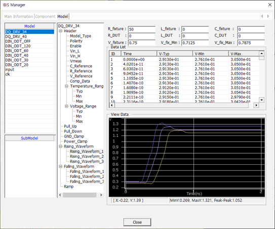
Click the Model tab menu, select
DQ_DRV_34.
You can find and review the AC/DC properties by clicking each
parameter of the DQ_DRV_34 model. By exploring the buffer’s AC/DC
characteristics, you can choose the proper buffer model for PI
Analysis.Figure 16.
Click Close to close the IBIS
Manager dialog.
Click OK to close the
dialog.
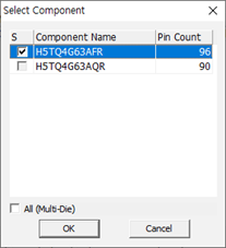
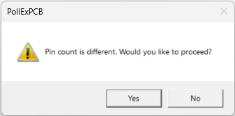
When the IBIS file has multiple components, the Select
Component dialog opens. Select one of them. Pin count is
a good reference to select the correct one.
Select the first component, click OK to close the Select
Component dialog.
Figure 17.
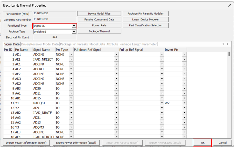
The Electrical & Thermal Properties
dialog opens. The DDR3 device’s part properties are assigned
automatically as shown in the Electrical & Thermal
Properties dialog.
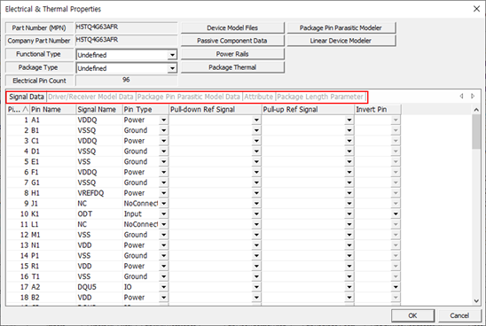
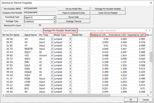
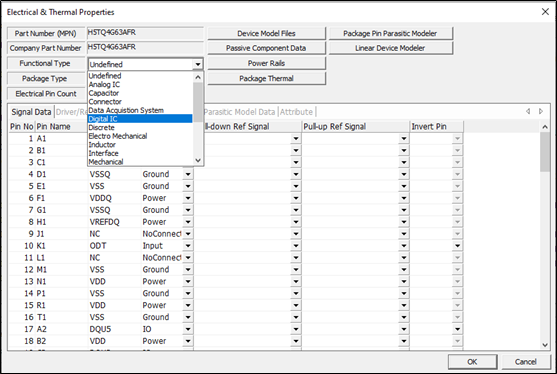
Select one of the tab menus among Signal Data, Driver/Receiver Model
Data, Package Pin Parasitic Model Data, and Attribute, to display
detailed information.
Figure 18. The Signal Data tab menu shows basic information such as Signal
Name, Pin Type, Pull-down/Pull-up Ref Signal, and Inverted Pin
status.
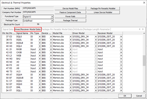
Select the Driver/Receiver Model Data tab menu to verify the detailed
information related to I/O buffer assignment for each pin included in
the IC part.
The Device Model column denoted as IBIS means that the pin’s model is
defined from IBIS data is not from SPICE or Linear Device Model. Set the
driver and receiver buffer model of the corresponding pin in the Driver
Model and Receiver Model columns. The Buffer Model specified here is
used as the Default Buffer Model when performing Network Analysis in the
future. The detailed AC/DC characteristics for each Driver/Receiver
Models can be reviewed in the Device Model Files
dialog.Figure 19. Figure 20.
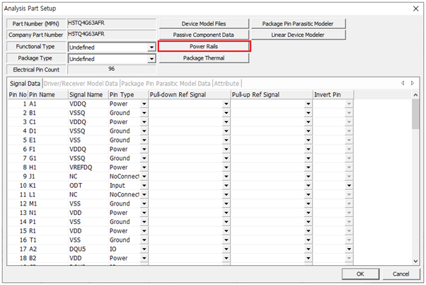
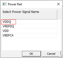
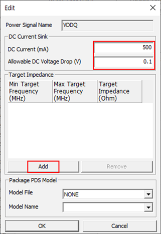
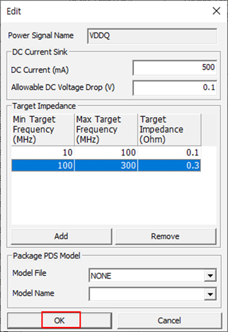
Setup Power Information.
Click Power Rails.
Figure 21.
The Power Rail dialog displays. All of the
power rails used for this component display in the middle of this
dialog.
Select Digital IC from the drop-down menu of
Functional Type field.
Figure 25.
Click OK to close the
Electrical & Thermal Properties
dialog.
The Electrical icon of H5TQ4G63AFR appears.Figure 26.
Assign IBIS to Controller
In this step, you will assign IBIS to controller using method 1.
From the menu bar, click Properties > Parts.
Applying the IBIS file follows the same steps as the previous step.
Double-click IC-NXP4330 and select the IBIS file
(C:\ProgramData\altair\PollEx\<version>\Examples\Solver\PI\Simulation_Model\CPU.ibs)
Click OK in the
Device Model Files dialog.
The following message will be displayed:Figure 27.
Click Yes.
Select Digital IC from the drop-down menu of Functional
Type field.
Click OK to close the
Electrical & Thermal Properties dialog.
Figure 28.
Assign Function Type
In this step, you will assign function type to power component.
To perform PI analysis, assign a power source component. If the Function Type of a
component is Connector or Power, the PollEx PI considers
this component as a power source.
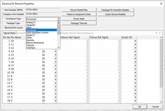
Double-click 47151-0001.
The Electrical & Thermal Properties dialog
displays.
Select Connector for the Functional Type.
Figure 29.
Click OK to close the
Electrical & Thermal Properties dialog.
Double-click 675031020.
For Functional Type, select Connector.
Assign Passive Component Data
In this step, you will assign passive component data to R and C.
Double-click the passive part and assign the proper values in the Passive
Component Data dialog depending on the selected Model Type.
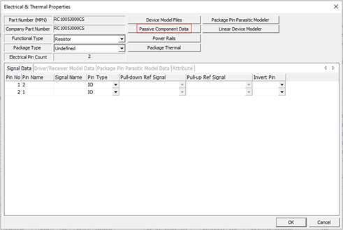
Double-click RC1005J000CS in the
Parts dialog.
The Electrical & Thermal Properties dialog
displays.Figure 30. Figure 31.
Click Passive Component Data in the Electrical
& Thermal Properties dialog.
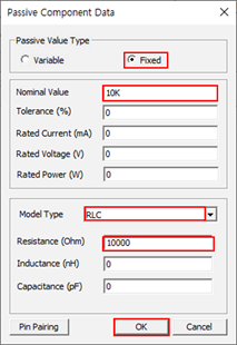
For Passive Value Type, select Fixed.
Note: In PI Analysis for Passive Value Type, it always
operates as a fixed type regardless of whether the variable type is selected
or not.
Enter 10K for the Nominal Value.
Leave the Model Type as RLC and enter 10000 for the
Resistance (Ohm).
Figure 32.
Click OK to close Passive Component Data dialogs.
Click OK to close the Electrical & Thermal Properties dialog
and return to Parts dialog.
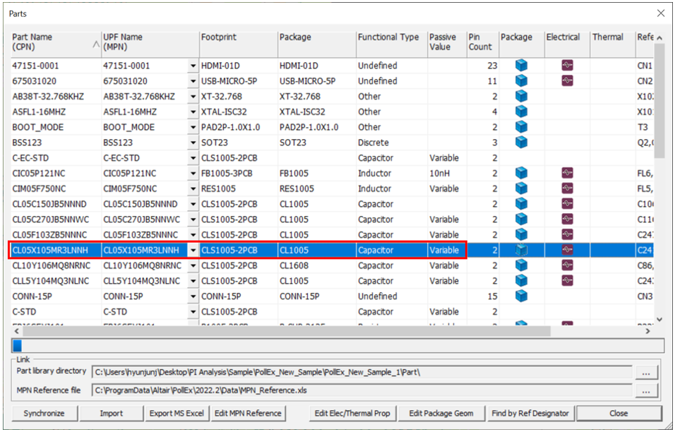
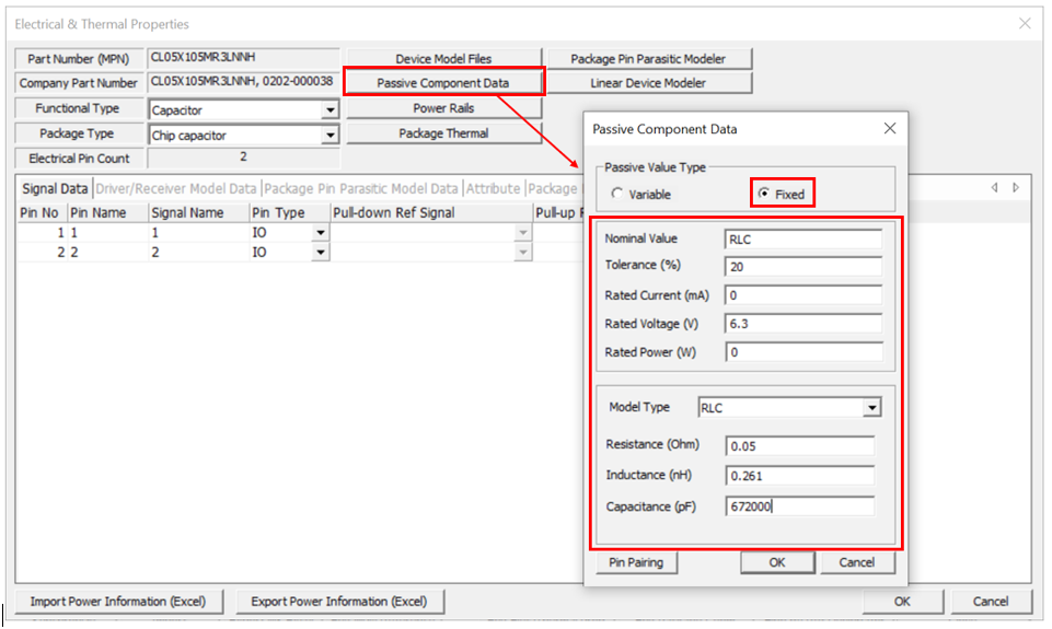
Double-click CL05X105MR3LNNH in the Parts dialog.
The Electrical & Thermal Properties dialog displays.
For Passive Value Type, select Fixed.
Enter RLC for the nominal Value and enter 20 and 6.3 for
tolerance and rate voltage.
Leave the model type as RLC and enter 0.05, 0.261 and 672000 for
Resistance, Inductance and Capacitance respectively.
Click OK to close Passive Component Data dialog.
Double-click CL05C270JB5NNWC in the Parts dialog.
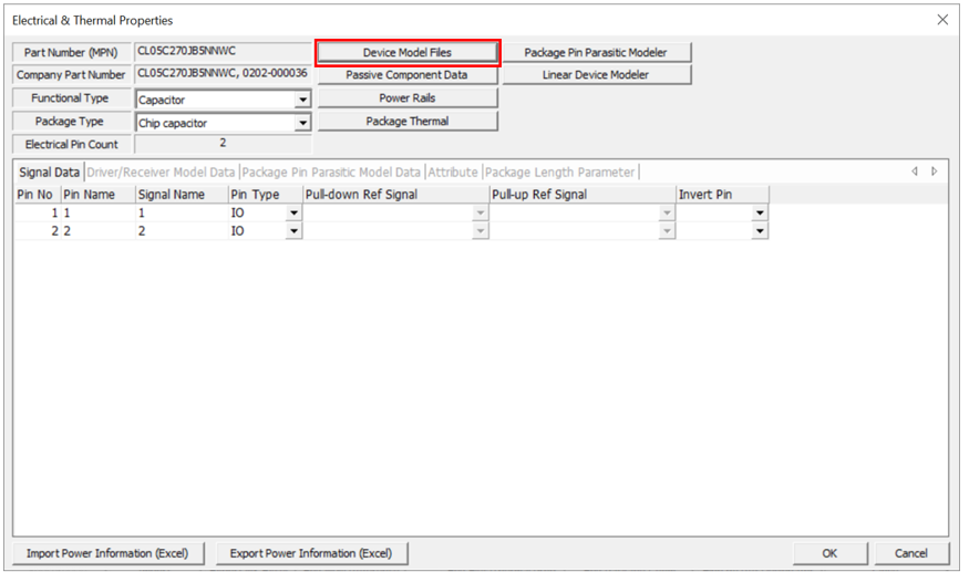
The Electrical & Thermal Properties dialog displays.
Assign Simulation Model (Spice) to CL05C270JB5NNWC.
Click Device Model Files.
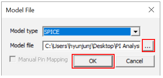
The Device Model Files dialog opens.
Click Add in the Device Model
Files dialog
The Model File dialog opens.
Click […] button to search and select the SPICE
file
([C:\ProgramData\altair\PollEx\<version>\Examples\Solver\PI\Simulation_Model\GRM153R60J105ME15_DC0V.mod)
for the capacitor and click Open.
Click OK to close the Model
Files dialog.
Click Passive Component Data in the
Electrical & Thermal Properties
dialog.
For Passive Value Type, select Fixed.
Enter SPICEfor the nominal Value and enter 20
and 50 for tolerance and rated voltage.
Leave the model type as SPICE and select
GRM153R60J105ME15_DC0V.mod for Model File and Model
Name.
Click OK to close Passive Component
Data dialog.
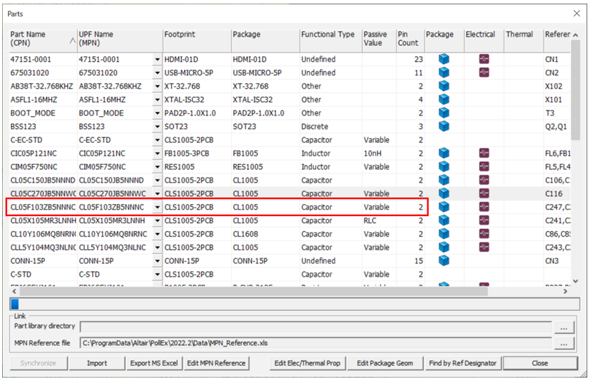
Return to Pars dialog and double-click
CL05F103ZB5NNNC in the Parts
dialog.
Assign Simulation model (S-Parameter) to CL05F103ZB5NNNC
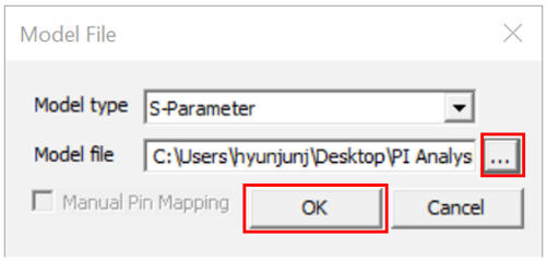
Click Device Model Files.
The Device Model Files dialog
opens.
Click Add in the Device Model
Files dialog. The Model File dialog
opens.
Click […] to search and select the S-Parameter
file
(C:\ProgramData\altair\PollEx\<version>\Examples\Solver\PI\Simulation_Model\GRM153R60J105ME15_DC0V.s2p)
for the capacitor and click Open.
Click OK to close the Model
Files dialog.
Click Passive Component Data in
Electrical & Thermal Properties
dialog.
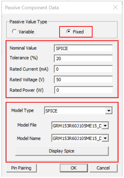
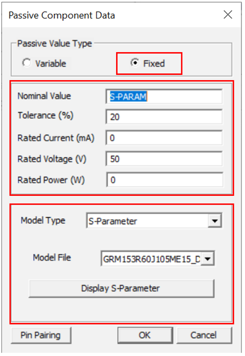
For Passive Value Type, select Fixed.
Enter S-PARAM for the nominal Value and enter
20 and 50 for tolerance and rated voltage.
Leave the model type as S-Parameter and select
GRM153R60J105ME15_DC0V.s2pfor Model File and Model
Name.
Click OK to close Passive Component
Data dialog.
Click OK to close Electrical & Thermal
Properties dialog
You can check the changed passive value in Parts
dialog.
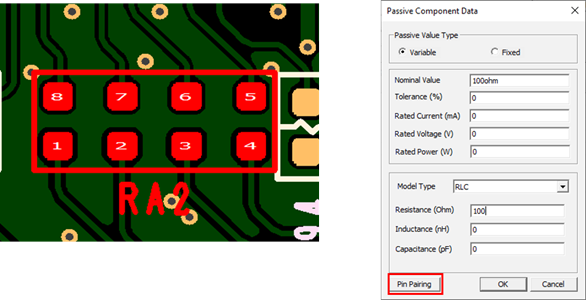
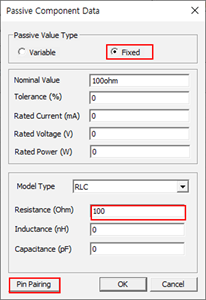
Continuously, Double-click the RA1005J000CS part that
has more than two pins in the Parts Dialog.
Figure 33.
Click for the Functional Type and select Resistor.
Click Passive Component Data in the Electrical
& Thermal Properties dialog.
For Passive Value Type, select Fixed.
Enter 100 ohm for the Resistance.
Figure 34.
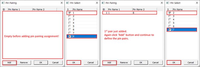
Click Pin Pairing in the Passive Component
Data dialog to open the Pin Pairing
dialog.
Click Add to define pin pairs.
The specified passive component values are assigned separately to these paired
pins.
(Pin pair : 1-8, 2-7, 3-6, 4-5)
Figure 35.
Close any opened dialogs.
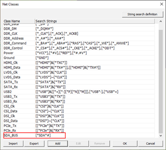
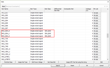
Add New Class Item
From the menu bar, click Properties > Net Classes.
The Net Classes dialog opens.
Click Add.
The ADD dialog opens.
For net Class name, enter SDA_BUS and enter search
string *SDA*# in the Search Strings field.
Figure 36.
Click Add String.
Click OK to close the
ADD dialog.
The SDA_BUS net class is registered in the Net
Classes dialog.
Click OK to close the
Net Classes dialog.
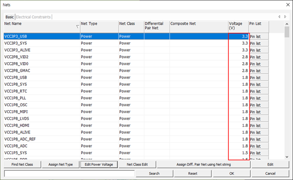
Click Properties > Nets.
The Nets dialog opens.
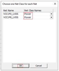
Click Find Net Class to assign net class using a
pre-defined net class file.
If there is a net whose net class is redundantly among the nets, the
Choose one Net Class for each Net dialog open.
Leave the Net Class Names as Power and click OK.
Figure 37.
Three nets are classified as the SDA_BUS net class.Figure 38.
Click OK to close the
Nets dialog.
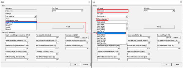
Assign Net Properties for Differential Pairs
In the Nets dialog there are two ways to assign the net
property.
Double-click MCU_ACK.
The Edit dialog displays.
Change Net Type to Diff Signal +.
Select the other pair net MCU_ACKB as Diff Signal using
the scroll bar.
Figure 39.
Click OK to close the
Edit dialog.
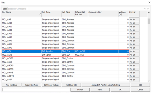
The MCU_ACK and MCU_ACKB nets are combined as a differential pair
net.Figure 40.
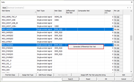
Select MCU_NADQS0 and MCU_PADQS0
in the Nets dialog.
Select Generate Differential Pair Net from the context menu.
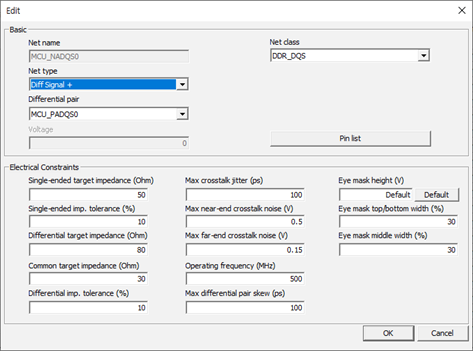
The Edit dialog opens.Figure 41.
Click OK to close the
Edit dialog.
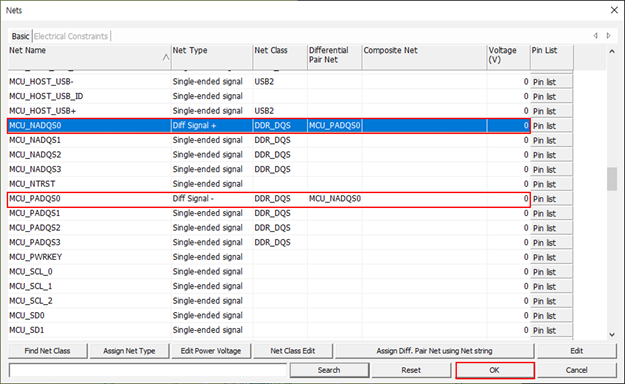
The MCU_NADQS0 and MCU_PADQS0 nets are combined as a differential pair
net.Figure 42. Figure 43.
Click OK to close the
Nets dialog.
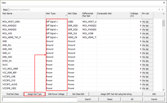
Assign Net Properties Automatically
From the menu bar, click Properties > Nets.
The Nets dialog opens.
Click Assign Net Type.
The PollEx PI sets the properties for all nets automatically using net
information described in IBIS files and property.Figure 44.
Click OK to close the
Nets dialog.
Assign Net Properties for Power
From the menu bar, click Properties > Nets.
The Nets dialog opens.
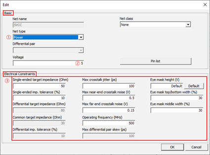
Double-click 5VCC.
The Edit dialog opens.
For Net Type, click Power.
For voltage, enter 5.0.
Click OK to close the
Edit dialog.
Figure 45.
Double-click VCC1P0_CORE.
For Net Type, select Power.
For voltage, enter 1.0.
Click OK to close the
Edit dialog.
Assign power value for power nets again using a different method.
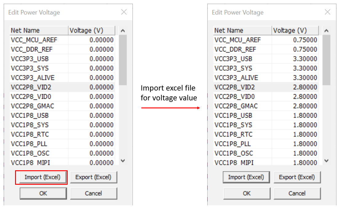
Click Edit Power Voltage.
The Edit Power Voltage dialog
opens.
Click import for the voltage value by using voltage_value.xlsx.
(File's path is below)
Or, Click each Voltage(V) field and enter the Power value of each power
net.
Figure 46.
Click OK to close the
Edit Power Voltage dialog.
The power values are assigned.Figure 47.
Click OK to close the
Nets dialog.
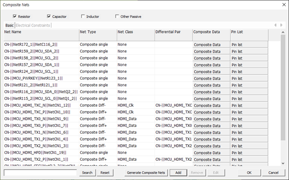
Make Composite Net
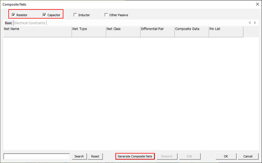
From the menu bar, click Properties > Composite Nets.
Activate Resistor and
Capacitor.
Click Generate Composite Net.
Figure 48.
The Selects Nets to Exclude dialog
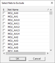
opens.
Specify nets that should not be composited with other nets, such as Power and
Ground nets.
Nets whose Net Type is declared as Power or Ground are automatically excluded
from the list.Figure 49.
Click OK and check the listed
composited nets.
Figure 50.
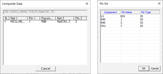
Click Composite Data or Pin List
to review composite net structure or the pin list.
Figure 51.
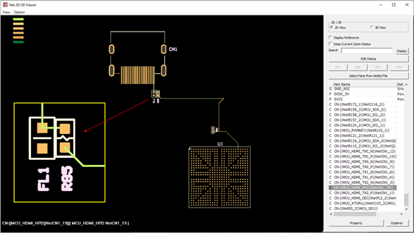
Note: If you want to check the total net composition
status for the composited nets, use the Option > Net 2D/3D Viewer menu. Select the composite net
CN-||MCU_HDMI_HPD||NetCN1_19||. The secondly
listed composited net above configured with MCU_HDMI_HPD and NetCN1_19
displays at the beginning of this composite net chapter.
Figure 52.
Click OK to close the
Composite Nets dialog.
In the PCB window, click File > Save to save the current setup.
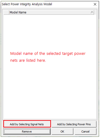
Assign Target Power Net
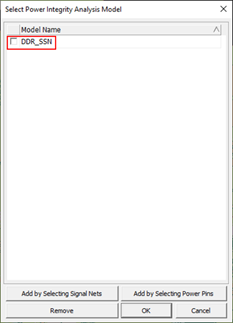
From the menu bar, click Analysis > Power Integrity.
The Select Power Integrity Analysis Model dialog
displays.
Click Add by Selecting Signal Nets.
Figure 53.
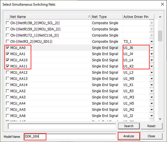
The Select Simultaneous Switching Nets dialog
displays. When selecting signal nets, the driver component of the Active Driver
pin item must be the same.
Select DDR address nets to analyze SSN.
Enter DDR_SSN as the new model name.
Figure 54.
Click Analyze to generate the PI model.
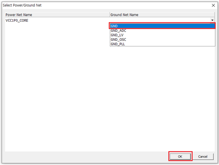
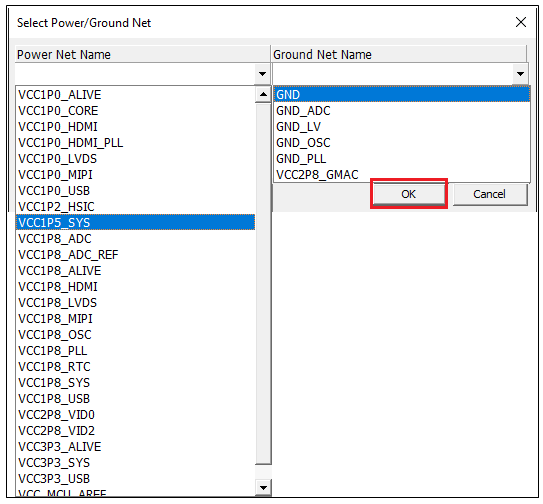
The Select Power/Ground Net dialog
opens.
Select the required power net and ground net and click OK.
In this sample design, the VCC1P5_SYS power supplies power to the DDR pins.
And GND is ground for DDR pins.Figure 55.
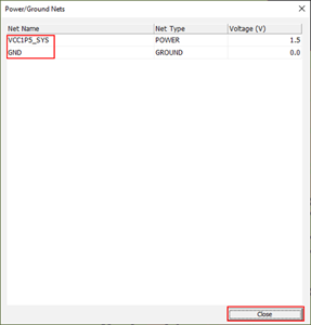
The Power Integrity Analyzer dialog for DDR_SSN
displays.
Click Properties > Power/Ground Nets.
The Power/Ground Nets dialog opens. The net
VCC1P5_SYS power net is selected for this analysis.
Click Close to close the Power/Ground
Nets dialog.
Figure 56.
Analyze PI using the Power Integrity Analyzer window.
From the menu bar, click File > Exit to close the Power Integrity
Analyzer dialog.
In the PollEx PCB window, click Analysis > Power Integrity from the menu bar.
The Select Power Integrity Analysis Model
dialog opens.Figure 57.
Click OK to close the
Select Power Integrity Analysis Model
dialog.
Select Required Power Net
In this step, you will select required power net to assign target power
net.
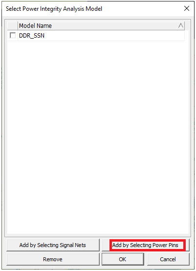
Click Analysis > Power Integrity to open the Select Power Integrity Analysis
Model.
Click Add by Selecting Power Pins to open the
Select Power Net Pins.
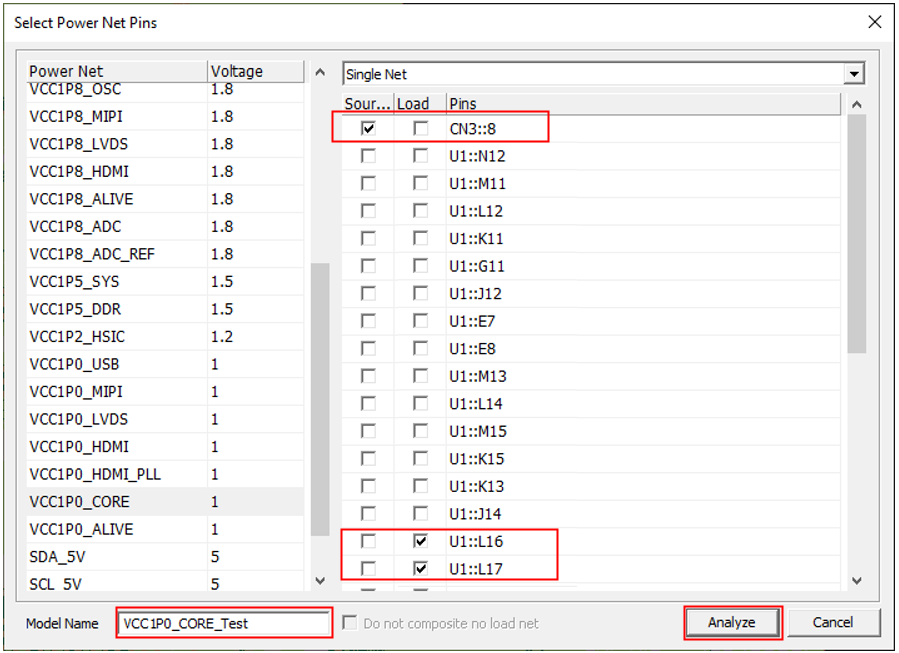
Figure 58. Select Power Integrity Analysis Model
Select VCC1P0_CORE from Power Net list
Select CN::8 pins for source component pins and select
U1_L17 and U1_L16 pins for
load component pins.
Figure 59. Select Power Net Pins
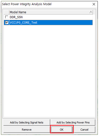
Enter VCC1P0_CORE_Test as the new model name.
Warning: If there is a space in the Model
name, the PDN analysis will fail.
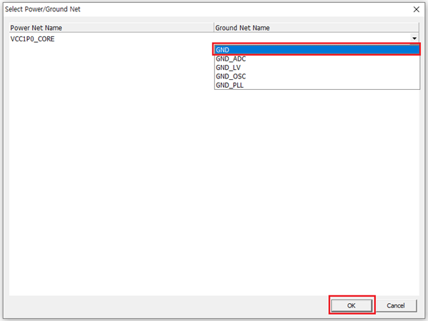
Click Analyze to generate the PI model.
The Select Power/Ground Net dialog
opens.
Select GND as a target ground net.
Figure 60. Select Power/Ground Net
Note: The Select Power/Ground
Netdialog is displayed only when the selected component has
multiple ground nets.
Click OK to close the
Select Power/Ground Net dialog.
The Power Integrity Analyzer dialog for VCC1P0_CORE
power net opens.
Note: You can review PI for VCC1P0_CORE
power net.
Click File > Exit to close the Power Integrity Analyzer
dialog.
Analyze DC IR-Drop
Click Analysis > Power Integrity.
The Select Power Integrity Analysis Model dialog
opens. You can see pre-saved PI models in the Model Name field. You can generate
a new PI model for analysis, however you will use the pre-saved PI
model.
Select VCC1P0_CORE_Test and click OK.
Figure 61.
The Power Integrity Analyzer dialog for
VCC1P0_CORE_Test PI model opens.
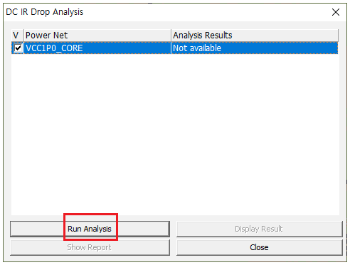
Click Analysis > DC IR Drop Analysis.
The DC IR Drop Analysis dialog opens.Figure 62.
Select VCC1P0_CORE and click Run
Analysis to start DC IR Drop analysis.
The DC IR Drop analysis starts. When the DC IR Drop analysis is done,
the DC IR Drop Analysis Result Display dialog
opens.
Select Voltage.
Figure 63. The voltage map displays. The VCC1P0_CORE power was 1.0V at the source pin
but dropped to 0.999V at the load pin.
Select Current Density.
Figure 64. The current density map displays.
Select Heat Density.
Figure 65. The power density map displays.
Select Voltage Drop.
Close DC IR Drop Analysis Result Display.
Figure 66.
Click Close to close the DC IR Drop
Analysis dialog.
Click to save this result.
Click File > Exit to close the Power Integrity Analyzer
dialog.
Analyze DC IR-Drop with Composite Net
Click Analysis > Power Integrity.
The Select Power Integrity Analysis Model dialog
opens. You can see pre-saved PI models in the Model Name field. You can generate
a new PI model for analysis, however you will use the pre-saved PI
model.
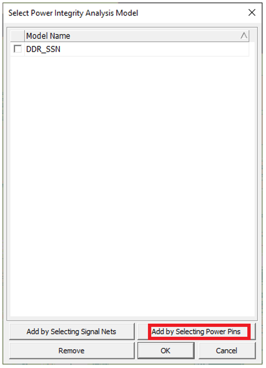
Click Add by selecting Power Pins.
Result : The Select Power Net Pins dialog opens.
Figure 67.
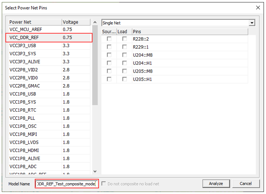
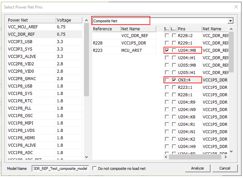
Select VCC_DDR_REF from Power Net list.
Enter VCC_DDR_REF_Test_composite model as a new model name.
Figure 68. Figure 69.
Select Composite Net type.
Select U204::M8 pin for source pin and selectCN3::4 pins for load
component pins.
Figure 70.
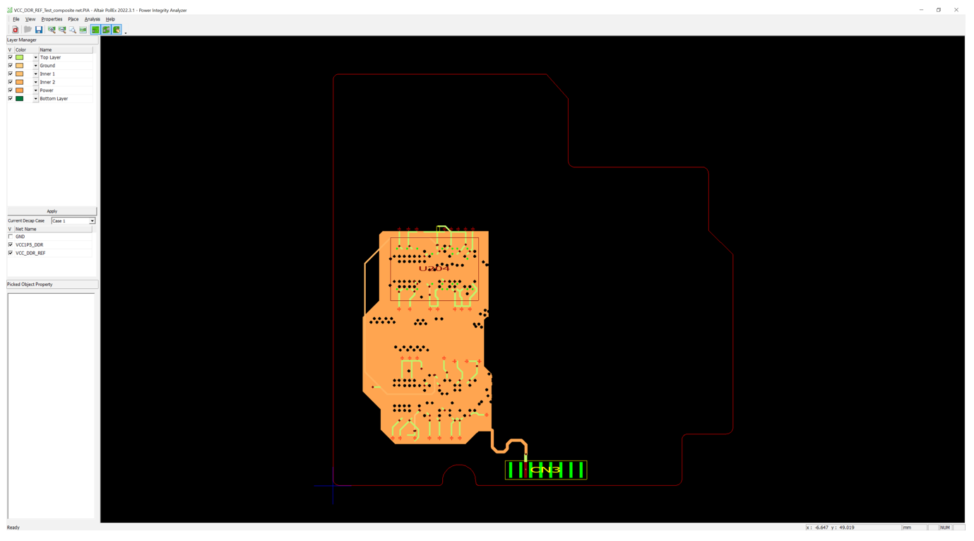
Click Analyze to generate the PI model.
The Power Integrity Analyzer dialog for VCC_DDR_REF
PI model opens.Figure 71.
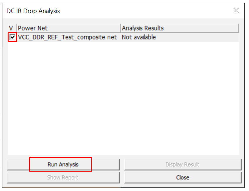
Click Analysis > DC IR Drop Analysis.
The DC IR Drop Analysis dialog opens.Figure 72.
Select VCC_DDR_REF and click Run
Analysis to start DC IR Drop analysis.
The DC IR Drop analysis starts. When the DC IR Drop analysis is done,
the DC IR Drop Analysis Result Display dialog opens. You
can check DC IR DROP Result involving the composite net type.Figure 73.
Analyze AC PDN
Click Analysis > Power Integrity.
The Select Power Integrity Analysis Model dialog
opens.
Select VCC1P0_CORE_Test and click OK.
Figure 74.
The Power Integrity Analyzer dialog for the
VCC1P0_CORE_Test PI model opens.
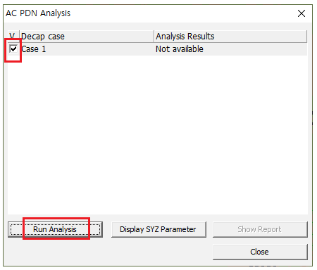
Click Analysis > AC PDN Analysis.
The AC PDN Analysis dialog opens.
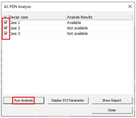
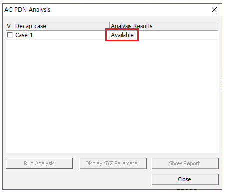
Select Case1 and click Run
Analysis to start AC PDN analysis.
Figure 75.
The AC PDN analysis starts. When the AC PDN analysis is done, the
Network Parameter Viewer opens. You can see whether the
Z11 meets Target Impedance.
Click Close to close the Network Parameter
Viewer dialog.
You can see the analysis result exists in the AC PDN
Analysis dialog for Case1.Figure 76.
Click Close to close the AC PDN
Analysis dialog.
Click to save this result.
Click File > Exit to close the Power Integrity Analyzer
dialog.
Analyze AC PDN - Create Test Case
The Z11 at some regions is higher than required. You can improve PDN results by
adding some decoupling capacitors, adding some VIAs or increasing the width of the
power/ground trace. In this tutorial, you will add some decoupling capacitors. Also,
for testing purposes, suppose that there is no decoupling capacitor in the
VCC1P0_CORE power source. By assigning the existing capacitor value as None.
PollEx PI makes it easy for you to compare the results
of various cases after creating different cases and assigning different conditions
to each case.
Note: User cannot place decoupling capacitors on top of Power
via. If they (de-cap and power via) overlap, error of AC PDN simulation may
occur.
Add Case.
Click Analysis > Power Integrity.
The Select Power Integrity Analysis Model
dialog opens.
Select VCC1P0_CORE_Test and click
OK.
Figure 77.
The Power Integrity Analyzer dialog for the
VCC1P0_CORE_Test model opens.
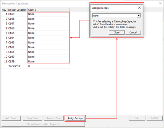
Click Properties > Decoupling Capacitors in the Power Integrity Analyzer
dialog.
The Decoupling Capacitors dialog opens. For
testing purposes, suppose that there is no decoupling capacitor in the
VCC1P0_CORE power source. By assigning existing capacitor value as
None.
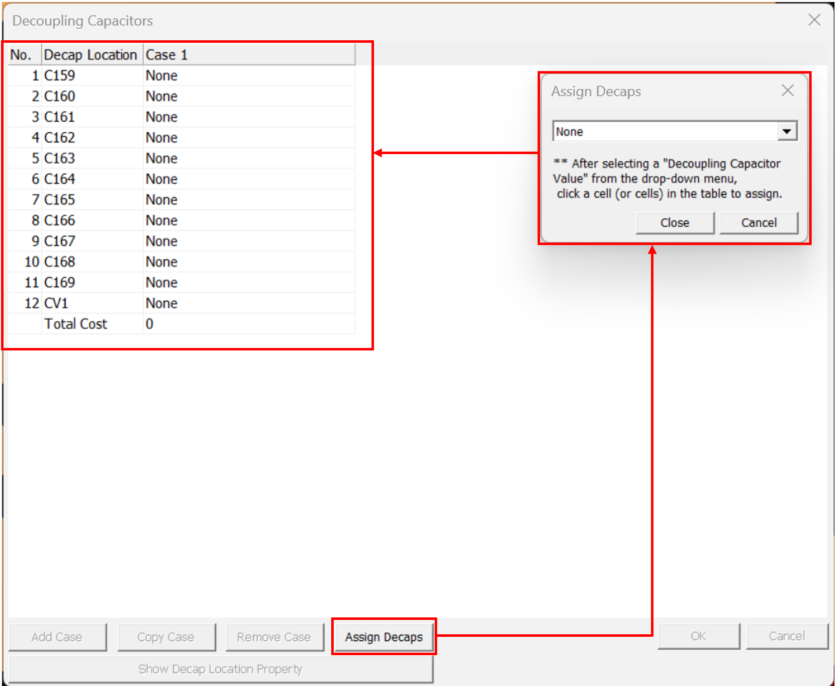
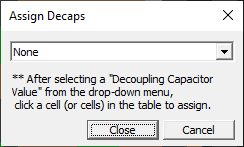
Click Assign Decaps to assign the capacitor
value for the current design.
The Assign Decaps dialog
opens.
Select None.
Figure 78.
Click C169~C159 to assign this value.
Click Close to close the Assign
Decaps dialog.
Figure 79.
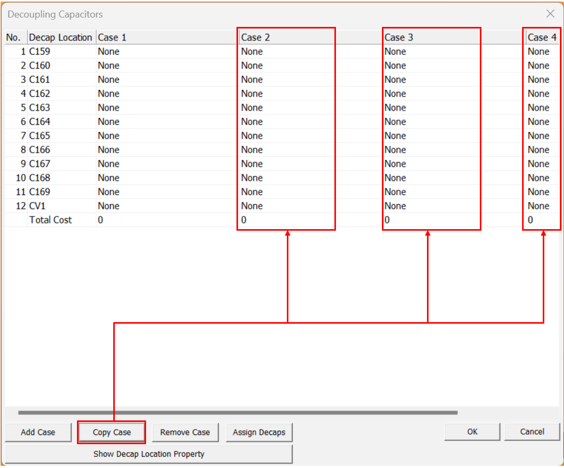
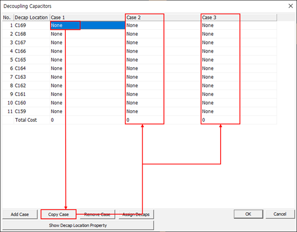
Add some test cases.
Click any component in the Case 1 column and click Copy
Case.
The Case 2 column is added.
Click any component in the Case 1 column and click Copy
Case.
The Case 3 column is added.Figure 80.
Click OK to close the
Decoupling Capacitors dialog.
Analyze AC PDN - Add Decoupling Capacitor
Add VRM capacitor.
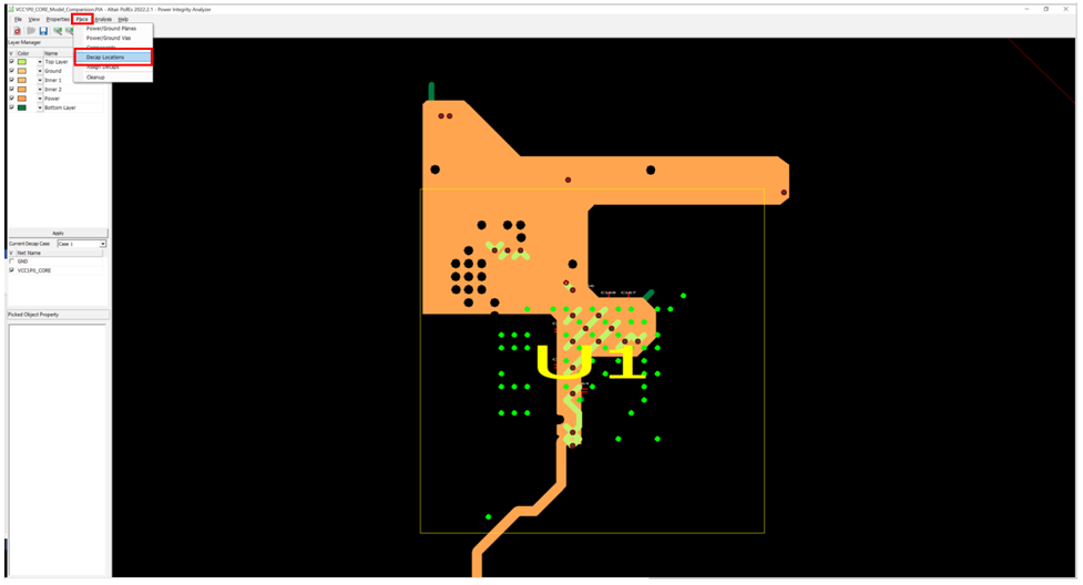
In the Power Integrity Analyzer dialog, execute
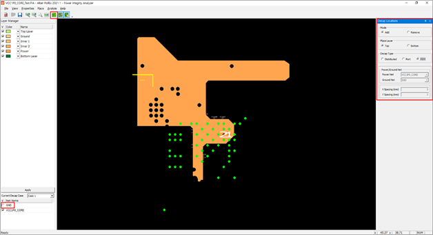
the Place-Decap Locations menu.
The Decap Locations field is added to the right side of
Power Integrity Analyzer dialog.
Unselect GND net for better view and turn-off
the display of trace by clicking .
You can see the VCC1P0_CORE net only. For a more accurate placement,
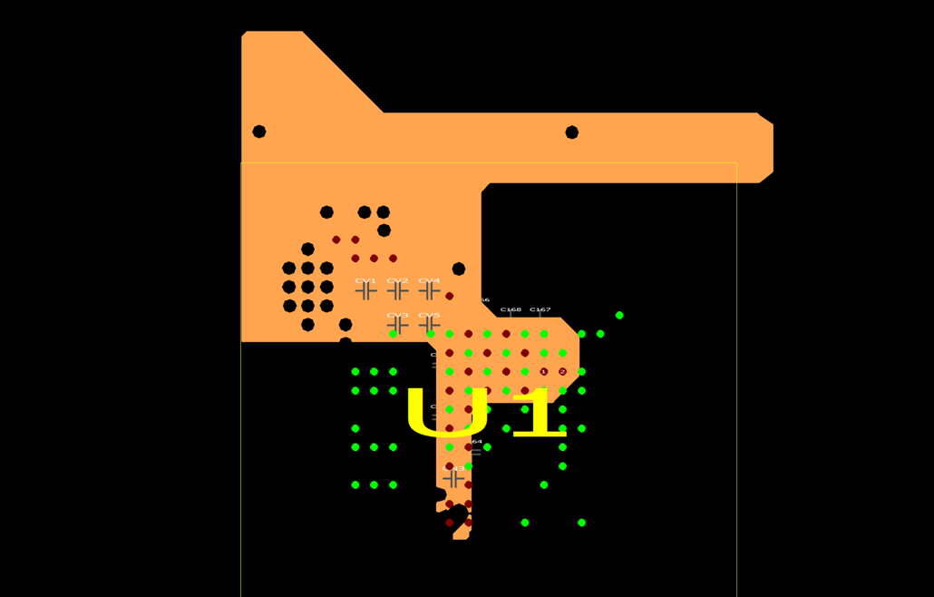
zoom in on the screen a bit.Figure 81. pi_unselect_gnd_net
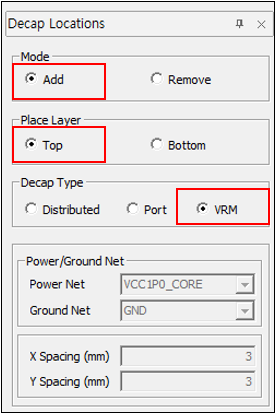
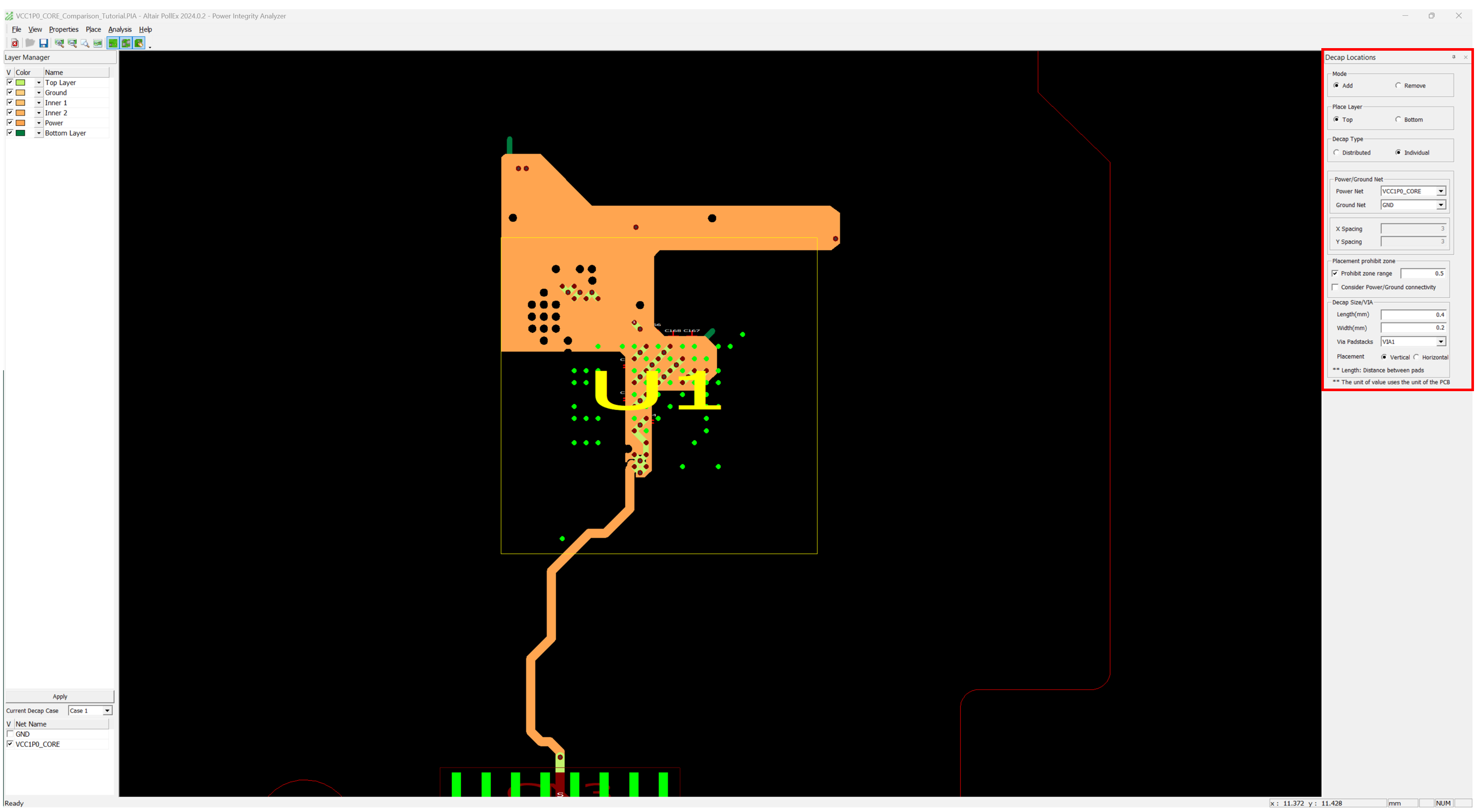
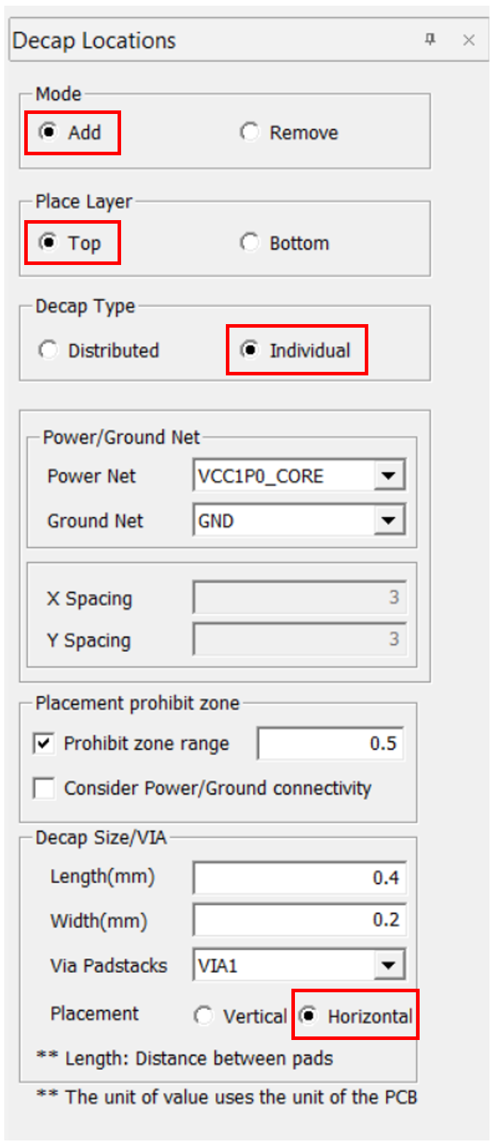
Select Add.
Select Top.
Select Individual.
Select Horizontal.
Figure 82.
Select the position (X:37.8, Y:21.8) where the
capacitor will be placed, near Source connector CN3.
The VRM capacitor with the name CN3 displays at that position. The
color of the CN3 capacitor is grey. It means that this capacitor only
has location information. After the value is assigned to the capacitor,
the color changes to red.Figure 83.
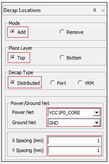
Add distributed capacitors.
Select Add.
Select Top.
Select Distributed.
Select VCC1P0_CORE for the Power Net.
Select GND for the Ground Net.
Enter 1.0 for X Spacing to set X axis spacing of
distributed capacitors.
Enter 1.0 for Y Spacing to set Y axis distance
of distributed capacitors.
Select Horizontal.
Figure 84. pi_add_distributed_capacitors
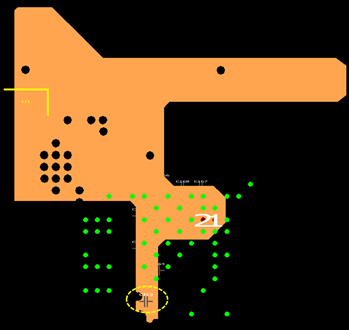
Use the mouse’s drag-drop function to distribute the capacitors near
the U1 component.
Drag Point: X: 37.00, Y:32.00 ~ X: 38.50, Y:29.50
The 6 distributed capacitors are placed. The coordinate of capacitors
is used as capacitor names.Figure 85.
Analyze AC PDN - Assign Decoupling Capacitor's Value
In case2, you will assign 10uF value for individual capacitor CV1. In case3, you will
assign 27pF property value for distributed capacitors.
There are two ways to assign the value of capacitor:
Using the Properties > Decoupling Capacitors.
Using the Place > Assign Decaps.
Assign value for individual capacitor CV1.
Click Properties > Decoupling Capacitors.
The Decoupling Capacitors dialog
opens.
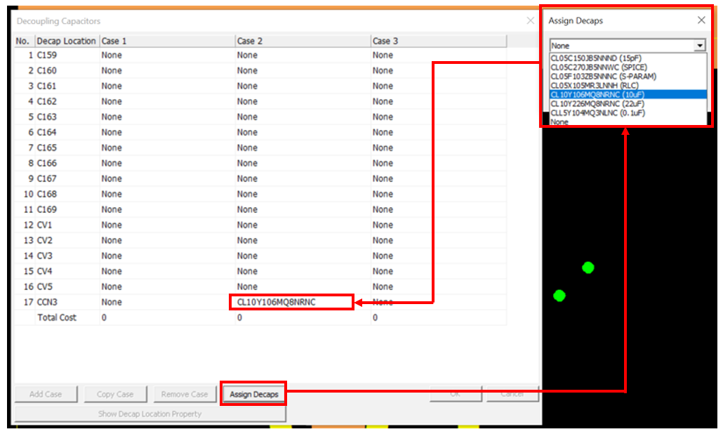
Click Assign Decaps.
The Assign Decaps dialog
opens.
Select CL10Y106MQ8NRNC (10uF).
Click the 18th line of Case2 column to assign this value.
The capacitor is assigned for 18th line of case2 column.Figure 86.
Click Close to close
the Assign Decaps dialog.
Click OK to close the
Decoupling Capacitors dialog.
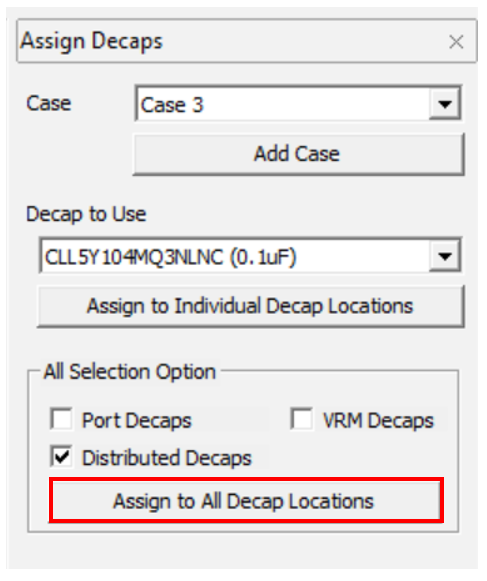
Assign property for distributed capacitors of case3.
Click Place > Assign Decoupling Capacitors.
The Decoupling Capacitors dialog
opens.
Click Assign Decaps.
Select CLL5Y104MQ3NLNC (0.1uF) for Decap to
Use.
Click the 12th~17th line of Case3 column to assign this value.
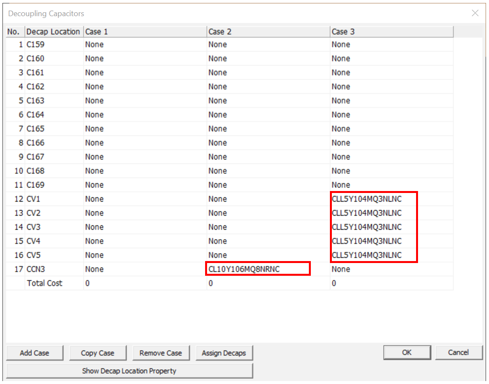
Figure 87.
The capacitor is assigned for 12th ~ 17th line of case3
column.
Review capacitor property.
Click Properties > Decoupling Capacitors.
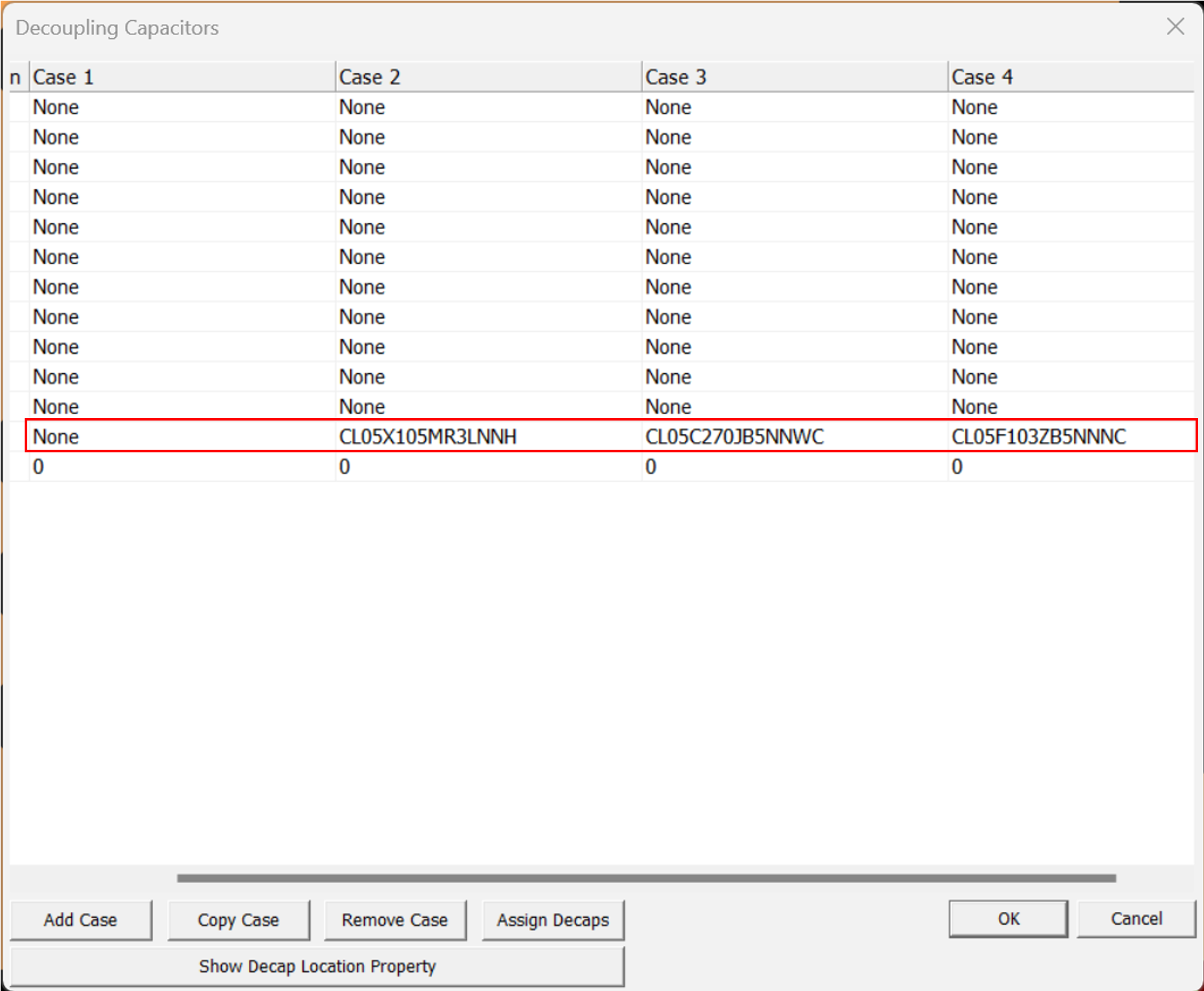
The Decoupling Capacitors dialog opens.Figure 88. You can review the capacitor assignment result.
Click OK to close the
Decoupling Capacitors dialog.
Click File > Save to save the current setup.
Run AC PDN Analysis
When you finish this step, you can compare PDN analysis results of Case1 (no
decoupling capacitor), Case2 (add 10uF VRM capacitor), and Case3 (add 27pF
distributed capacitors).
Click Analysis > AC PDN Analysis.
The AC PDN Analysis dialog opens.
Enable the Case 1, Case 2, and
Case 3 check boxes.
Click Run Analysis.
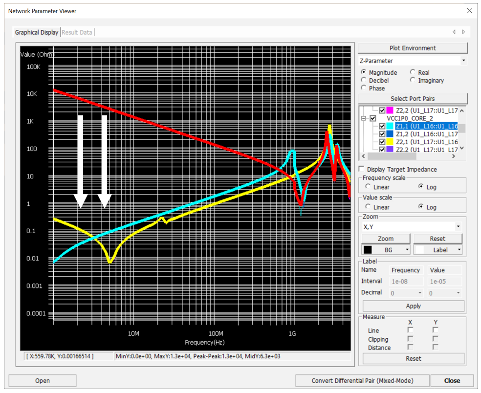
Figure 89. The AC PDN analysis starts. When the PDN analysis is done, the
Network Parameter Viewer dialog opens.
Turn on the waveform of U1_L16::U1_L16 (Z11) of each
case for comparison.
Change the wave colors.
Set Case1 to Red.
Set Case2 to Cyan.
Set Case3 to Yellow.
Figure 90. The 10uF low resonance frequency VRM capacitor is effective for improving
the characteristics of the low frequency band Z11, and 0.1uF high resonance
frequency distributed capacitors are effective for improving the characteristics
of the mid frequency band Z11.
Run AC PDN Analysis-Comparative RLC, SPICE, and S-Parameter
When you finish this step, you can compare PDN analysis results of RLC model, SPICE
model and S-Parameter model.
Click Analysis > Power Integrity.
The Select Power Integrity Analysis Model dialog
opens.
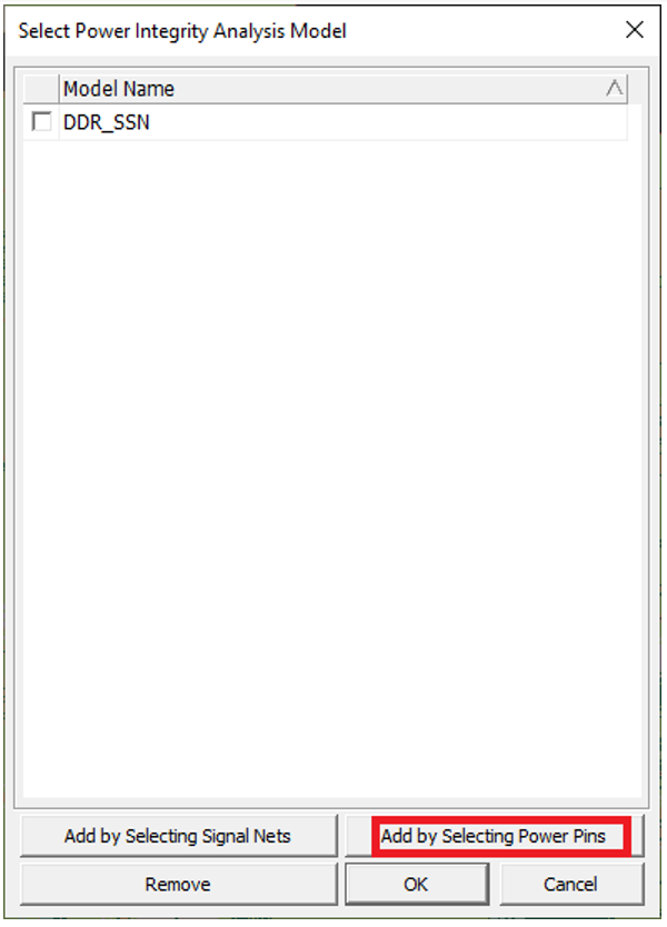
Click Add by Selecting Power Pins.
The Select Power Net Pins dialog opens.
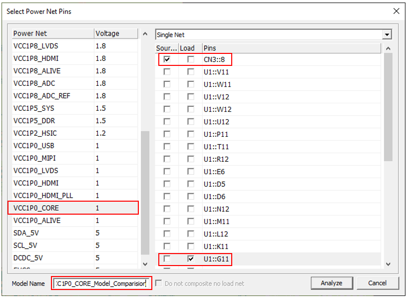
Select VCC1P0_CORE from Power Net list.
Select CN3::8 as source component pin and
U1::G11 pin for load component pins.
Enter VCC1P0_CORE_Model Comparison as the new model
name.
Figure 91.
Click Analyze to generate the PI model.
The Select Power/Ground Net dialog
opens.
Select GND as a target ground net.
The Select Power/Ground Net dialog is displayed
only when the selected component has multiple ground nets.
Click OK to close Select Source Pin
dialog.
The Power Integrity Analyzer dialog for VCC1P0_CORE
power net opens. You can review PI for VCC1P0_CORE power net.
Add Port capacitor.
Click Place > Decap Locations in the Power Integrity Analyzer
dialog.
The Decap Locations dialog opens.
For Mode, select ADD.
For Place Layer, select TOP.
For Decap Type, select Individual.
For Placement, select Horizontal.
Select the position (X:37.00,Y:29.00) where the capacitor will
be placed, near Port1 (G11). The Individual capacitor with the name
CV1 displays at that position. The color of the CV1
capacitor is grey.
Add cases.
Click Properties > Decoupling Capacitors in the Power Integrity Analyzer
dialog.
The Decoupling Capacitors dialog
opens.
Click Assign Decaps to assign the capacitor
value for the current design.
The Assign Decaps dialog
opens.
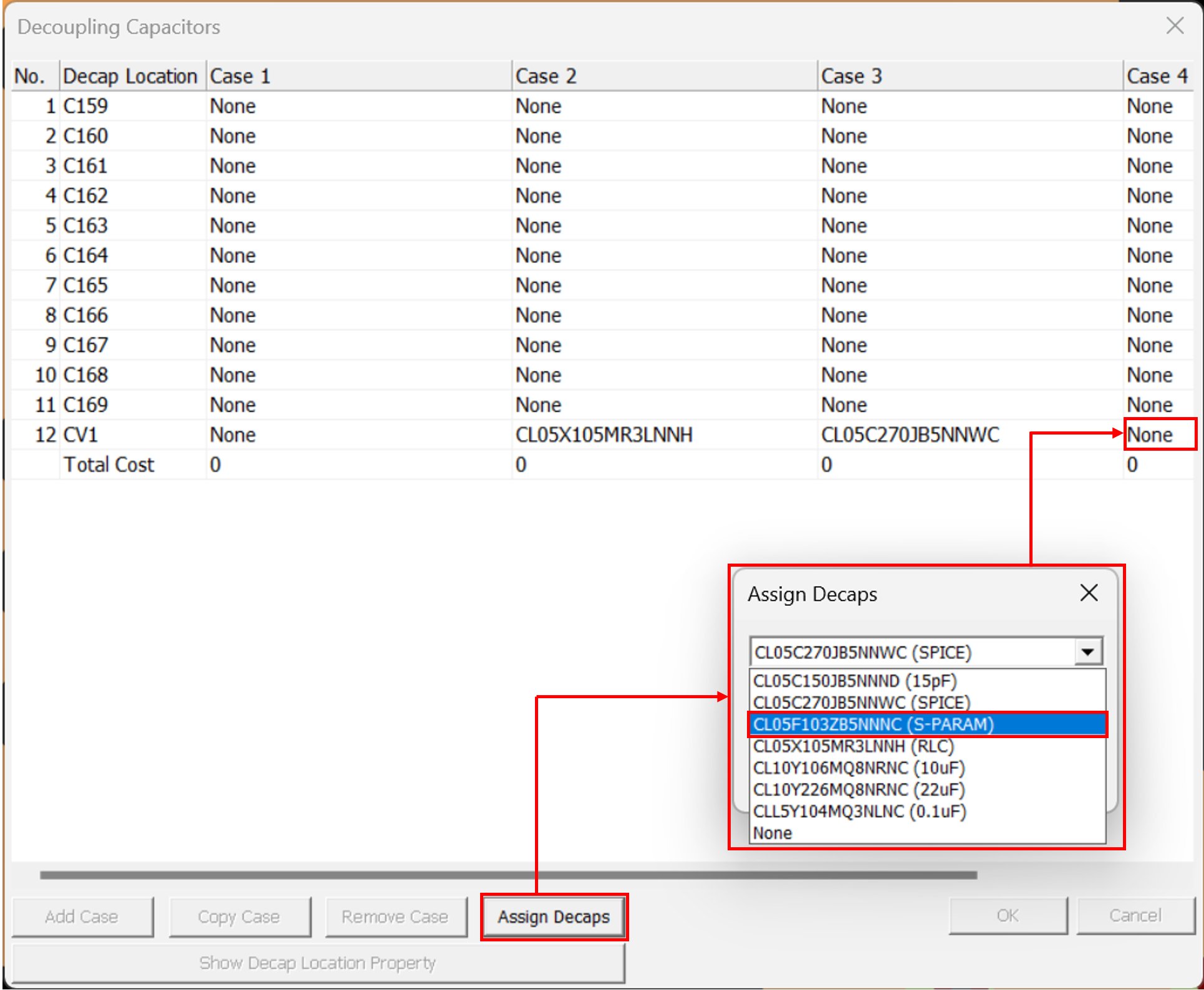
Select None.
Add some test cases.
Click any component in the Case 1 column and click Copy
Case.
The Case 2 column is added.
Click any component in the Case 1 column and click Copy
Case.
The Case 3 column is added.
Click any component in the Case 1 column and click Copy
Case.
The Case 4 column is added.
Assign value of Port capacitor for each Case 2,
Case 3, and Case 4.
Click Properties > Decoupling Capacitors in the Power Integrity Analyzer
dialog.
The Decoupling Capacitors dialog
opens.
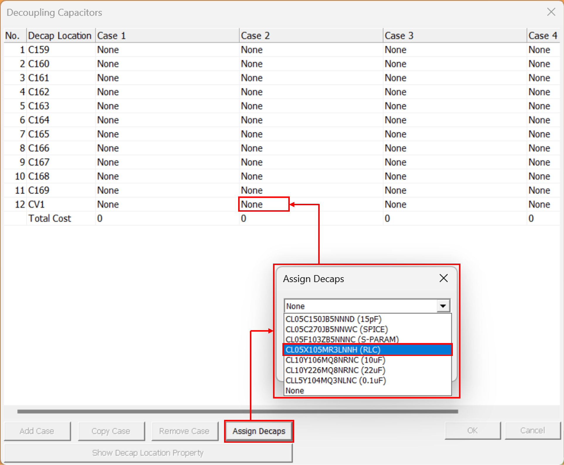
Click Assign Decaps.
The Assign Decaps dialog
opens.
Select CL05X105MR3LNNH (RLC)
Click the 1st line of Case 2 column to assign
this value. The capacitor is assigned for 1st line of Case
2 column.
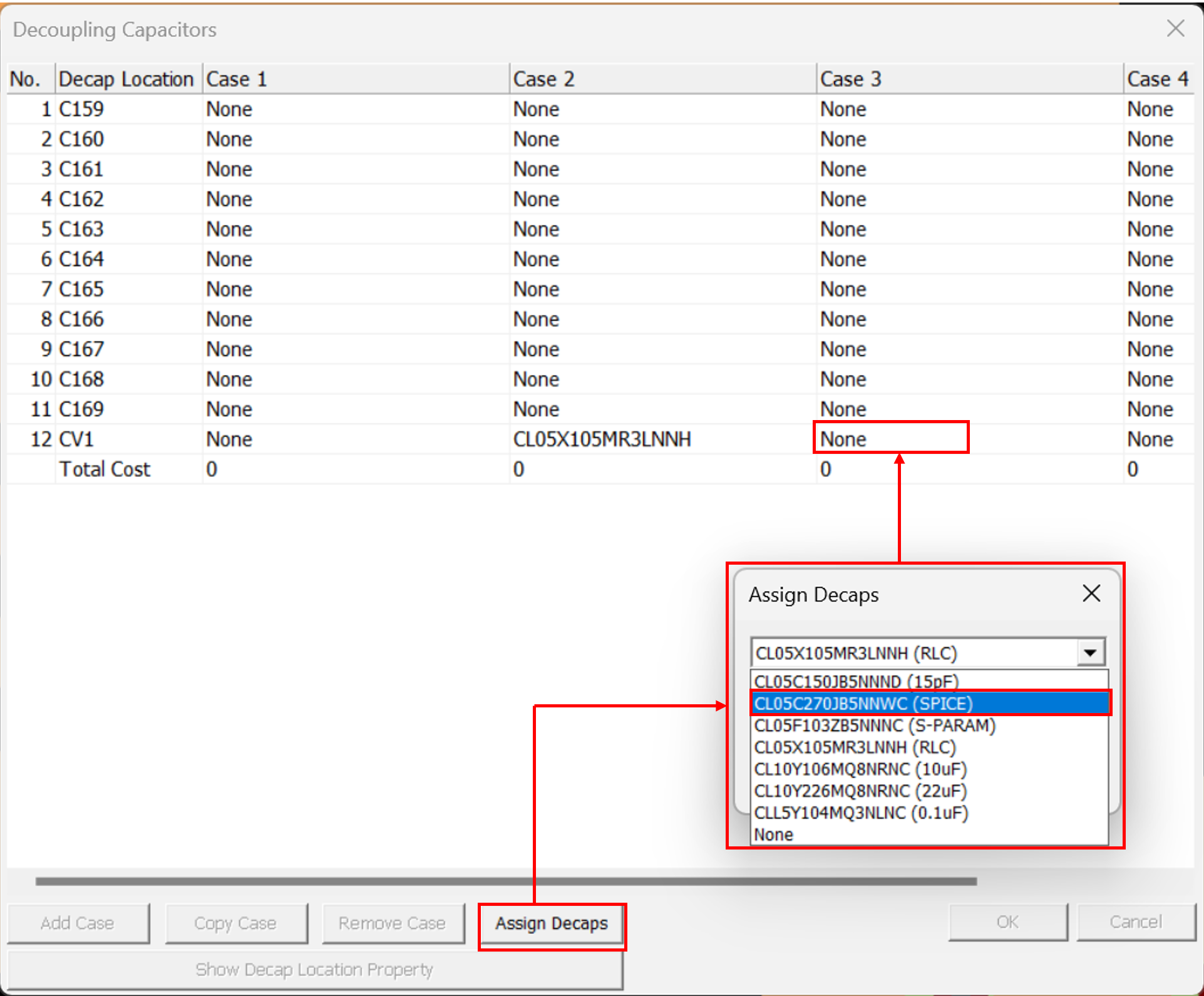
Select CL05C270JB5NNWC (SPICE).
Click the 1st line of Case 3 column to assign
this value. The capacitor is assigned for 1st line of Case
3 column.
Select CL05F103ZB5NNNC (S-PARAM).
Click the 1st line of Case 4 column to assign
this value. The capacitor is assigned for 1st line of Case
4 column.
Click OK to close the Assign
Decaps dialog.
Click OK to close the Decoupling
Capacitors dialog.
Click File > Save to save the current setup.
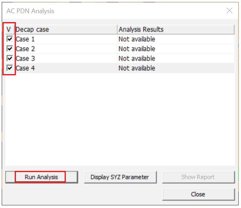
Click Analysis > ACPDN Analysis.
The ACPDN Analysis dialog opens.
Enable the Case 1, Case 2,
Case3, and Case 4 check
boxes.
Click Run Analysis.
The AC PDN analysis starts. When the PDN analysis is done, the
Network Parameter Viewer dialog opens.
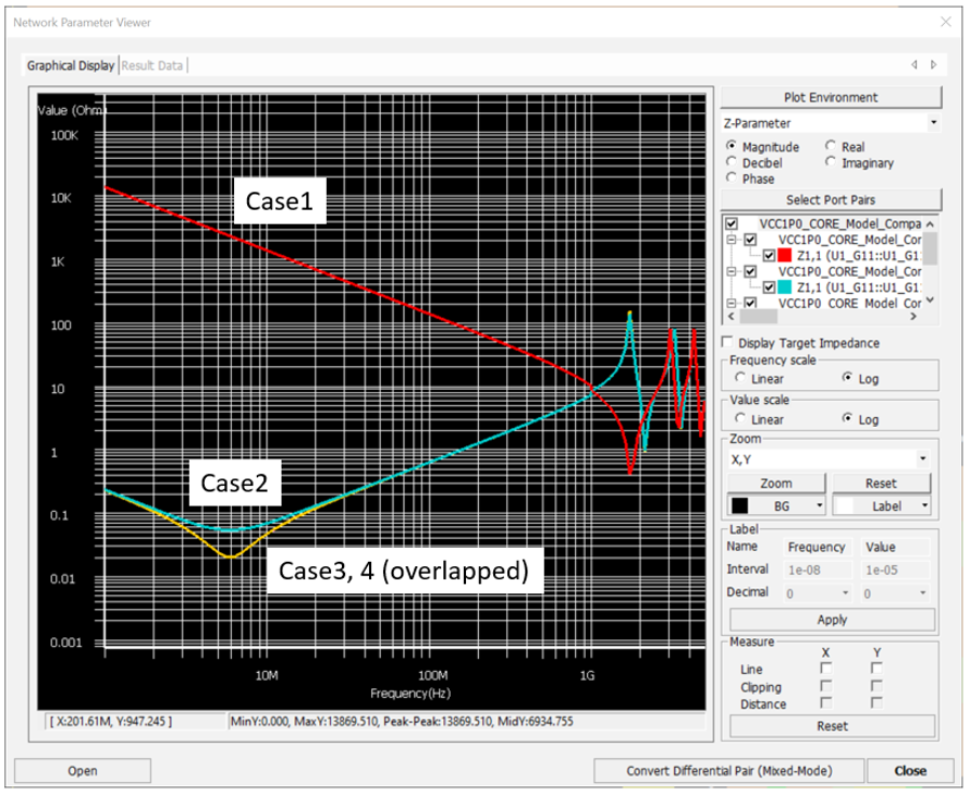
Change the wave colors.
Set Case1 to Red.
Set Case2 to Cyan.
Set Case3 to Yellow.
Set Case4 to Pink. (It is overlapped with Case3)
The 1uF low resonance frequency Port capacitor is effective for
improving the characteristics of the low frequency band Z11.
In case 3 and 4, we applied both the SPICE model and S-parameter
model of the GRM153R60J105ME15, and according to the
GRM153R60J105ME15 data sheet, it has a resonant frequency
of 10MHz. As a result, the AC PDN analysis shows that a resonance
point is formed at around 8MHz, which is close to the 10MHz resonant
frequency.

 and select
FR4.0.
The dielectric constant for TOP layer changes from 4.5 to 4.0.
and select
FR4.0.
The dielectric constant for TOP layer changes from 4.5 to 4.0.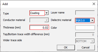
 to search and select the IBIS file
(C:\ProgramData\altair\PollEx\<version>\Examples\Solver\PI\Simulation_Model\Memory.ibs)
for DDR3 Memory device and click Open.
to search and select the IBIS file
(C:\ProgramData\altair\PollEx\<version>\Examples\Solver\PI\Simulation_Model\Memory.ibs)
for DDR3 Memory device and click Open.


 to save this result.

 .
You can see the VCC1P0_CORE net only. For a more accurate placement, zoom in on the screen a bit.
.
You can see the VCC1P0_CORE net only. For a more accurate placement, zoom in on the screen a bit.