Board
PCB Outline Spacing
Checks the clearance between board contour and placed package shape.
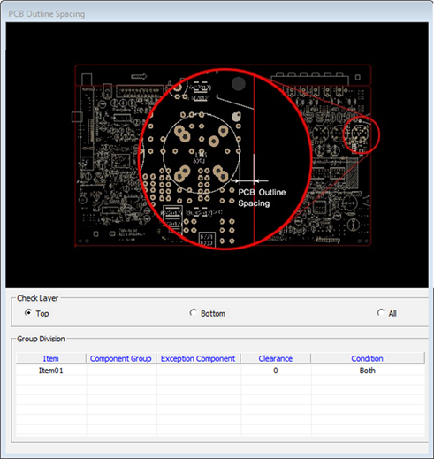
- Check Layer: Select checking target layer.
- Item: Input item name.
- Component Group: Specify checking target component group.
Figure 2. 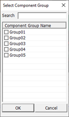
- Exception Comp: Specify checking-exception component group.
Figure 3.
- Clearance: Define the clearance distance between board contour and package.
- Condition: Select the measurement base for package.
- Both: Dimension including package body and lead.
- Body: Package body.
- Lead: Package lead.
Board Outline Spacing
Checks the clearance between array board contour and single board’s components.
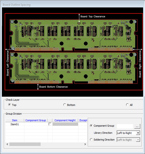
- Check Layer: Select checking target layer.
- Group Division
Figure 5. 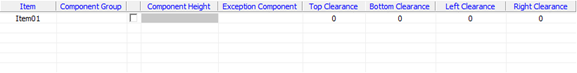
- Item: Input item name.
- Component Group: Specify target component group.
Figure 6.
- Component Height: Use the component with a height that is within the set
range as a checking target among selected components.
Figure 7. 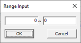
- Exception Component: Specify checking-exception component group.
Figure 8.
- Top Clearance: Define package clearance with array board’s top.
- Bottom Clearance: Define package clearance with array board’s bottom.
- Left Clearance: Define package clearance with array board’s left side.
- Right Clearance: Define package clearance with array board’s right side.
- Soldering Comp Group: If you use soldering direction component, specify the GROUP to define the direction.
- Soldering Direction: If soldering direction showing component is not used, you can directly define the direction of soldering.