Solder Mask Checker
Calculate solder quantity for wave soldering process.
-
From the menu bar, click .
The User Solder Mask dialog opens. You can see pad and solder mask on design.
-
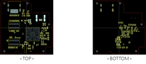
For View Setting, select top or bottom layer.
Solder quantity calculation is done for top or bottom, respectively. In DIP type component case placed on top layer, calculation is done for the bottom layer. Check the solder mask status of the bottom layer.
Figure 1. 
-
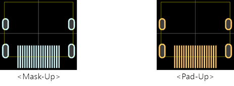
Select the display order of pad or solder mask.
Figure 2. 
- View list of components and pins.
-
Click Calculate to calculate solder mask areas for
layers and components.
Figure 3. 
- SMD Component Area: Total area summation of SMD pads.
Figure 4. 
- Condition: Only pad has solder mask.
- When solder mask is bigger than pad dimension: pad dimension = 1.2mm * 0.8mm.
- When pad is bigger than solder mask dimension: solder mask dimension = 1mm * 0.8mm.
- Calculate the dimension for solder mask and pad.
- DIP Component Area: Total area summation for PTH (plated through hole)
pad’s solder mask.
Figure 5. 
- Condition: Only for the bottom layer’s PTH pad that has solder mask.
- When solder mask is bigger than the pad dimension: pad dimension = (0.7mm)2 * π.
- When pad is bigger than solder mask dimension: solder mask dimension = (0.75mm)2 * π.
- Calculate the dimension for solder mask and pad.
- Board Figure: Total solder mask dimension for the board’s non-electric geometries.
- Total Area: The summation for the above three.
- SMD Component Area: Total area summation of SMD pads.
- Zoom In / Zoom Out / 1:1 Default View: Same as PollEx PCB.
-
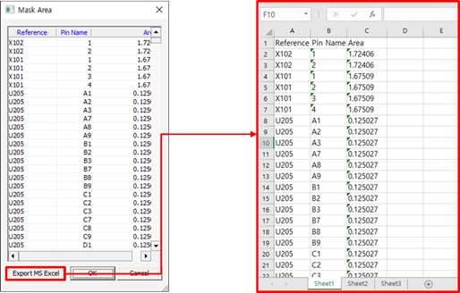
Display Solder Mask Area List: After getting each of the component’s solder
paste dimensions, export the results into a MS/Excel file (including top and
bottom layers).
Figure 6. 