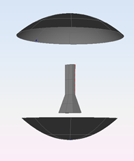
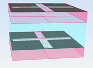
Input or set the antenna. Set the surface of the internal face of the radome. The
radome will be simulated by modelling this surface by a material surface.
Figure 1. Antenna and an internal surface of the radome layers.
If the material for modelling the radome is not available, add a new material for
modelling the radome layers and FSS. This material considers the
reflection/transmission coefficients. A file with these coefficients is obtained
using PERIODICAL STRUCTURE (PS) module with a unit cell that models the radome
layers/FSS , see Cell Menu
and Training Examples.
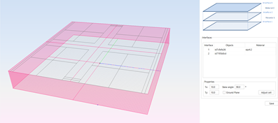
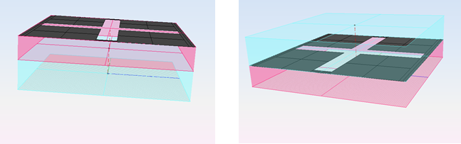
Figure 2. Example of the unit cell for modelling a radome surface composed by a
dielectric layer of 1.4 mm of thickness, of material epsilon 4.2 that has a
relative permittivity of 4.2 and is covered by a perfect electrical conducting
surface with a cross-slot. Unit cell dimensions: 10x10 mm. Cross dimensions:
total arms lengths = 9.25mm; wide = 1.20 mm. The upper face of the unit cell
(metal with cross slot) corresponds with the internal face of the radome
layer.
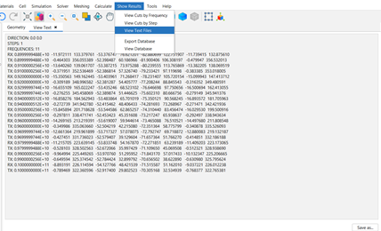
Get and output the Rx/Tx matrices in the PS module.
Figure 3. Save the file with the Rx/Tx matrices obtained in the frequency range from
9.0 to 10.0 GHz with 0.1 GHz Steps.
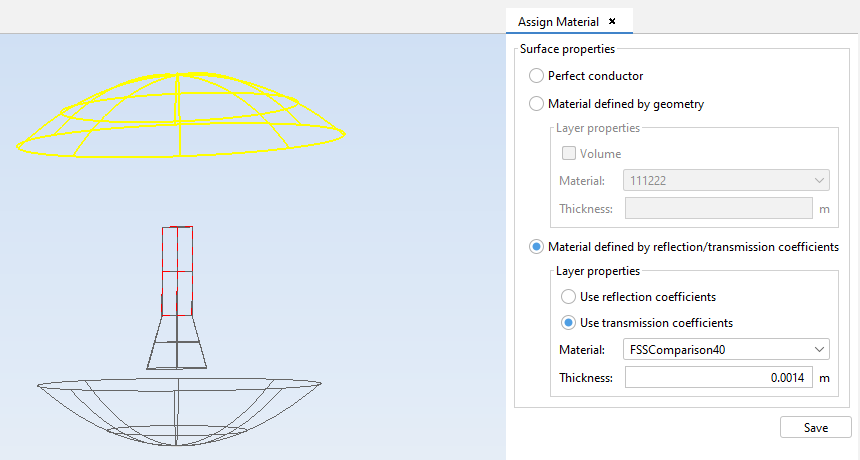
Define in MOM module a material with the Rx/Tx matrices generated in PS module. This
material must be saved for future simulations.
Figure 4. Assign the new material to the radome.
Select Use transmission coefficients and in the
Thickness field, set the thickness of the unit cell.
Mesh and run the case.Figure 5. Assign Material to the radome surface.
Define Radome by Several Material Surfaces
User has the option to split complex thick layers into two or more layers structures,
in such a way that these structures together compose the original structure. Figure 6 shows an example
of this splitting.Figure 6. Example of the unit cell for modelling a radome surface composed,
starting from the top by metal with cross slot, a dielectric layer of
epsilon 4.2 and thickness 1.4 mm, a layer of foam (relative permittivity
1.05) of 3.6 mm of thickness, metal with cross slot and in the bottom a
dielectric layer of epsilon 4.2 and thickness 1.4 mm. Notice that the total
height of the unit cell is 6.4 mm. The surface at the top of the cell
corresponds with the internal face of the radome.
Figure 7. The radome layers is split into two unit cells: Unit cell (a) in the left
is composed by, starting from the top by metal with cross slot, a dielectric
layer of epsilon 4.2 and thickness 1.4 mm and a layer of foam of 1.8 mm of
thickness; Unit cell (b) in the right composed by a layer of foam of 1.8 mm
of thickness, metal with cross slot and a dielectric layer of epsilon 4.2
and thickness 1.4 mm.
The radome structure is modeled by a set of material surfaces, each one of them
corresponding to a structure resulting from the splitting. Figure 8 shows the case of
the structure splitting of previous figures.Figure 8. The radome is modeled by two material surfaces. The lower surface, of
blue color has assigned a material that corresponds with unit cell (a) and
the upper surface, of maroon color, corresponds with unit cell (b).
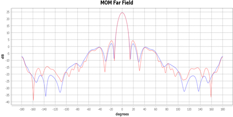
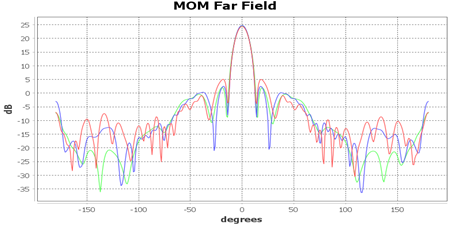
Figure 9 compares results
for radiation pattern cuts with and without the splitting of the radome
structure.Figure 9. Radiation pattern cut, phi=0, at 9.5 GHz of the antenna with radome
modeled by two material surfaces (red line), one material surface (blue
line) and the antenna alone (green line).