Altair PollEx 2023 Release Notes
This section contains all the changes for the 2023 release for PollEx.
Highlights
- The PCB menus have been reorganized to provide better clarity.
Figure 1. PCB menu reorganization 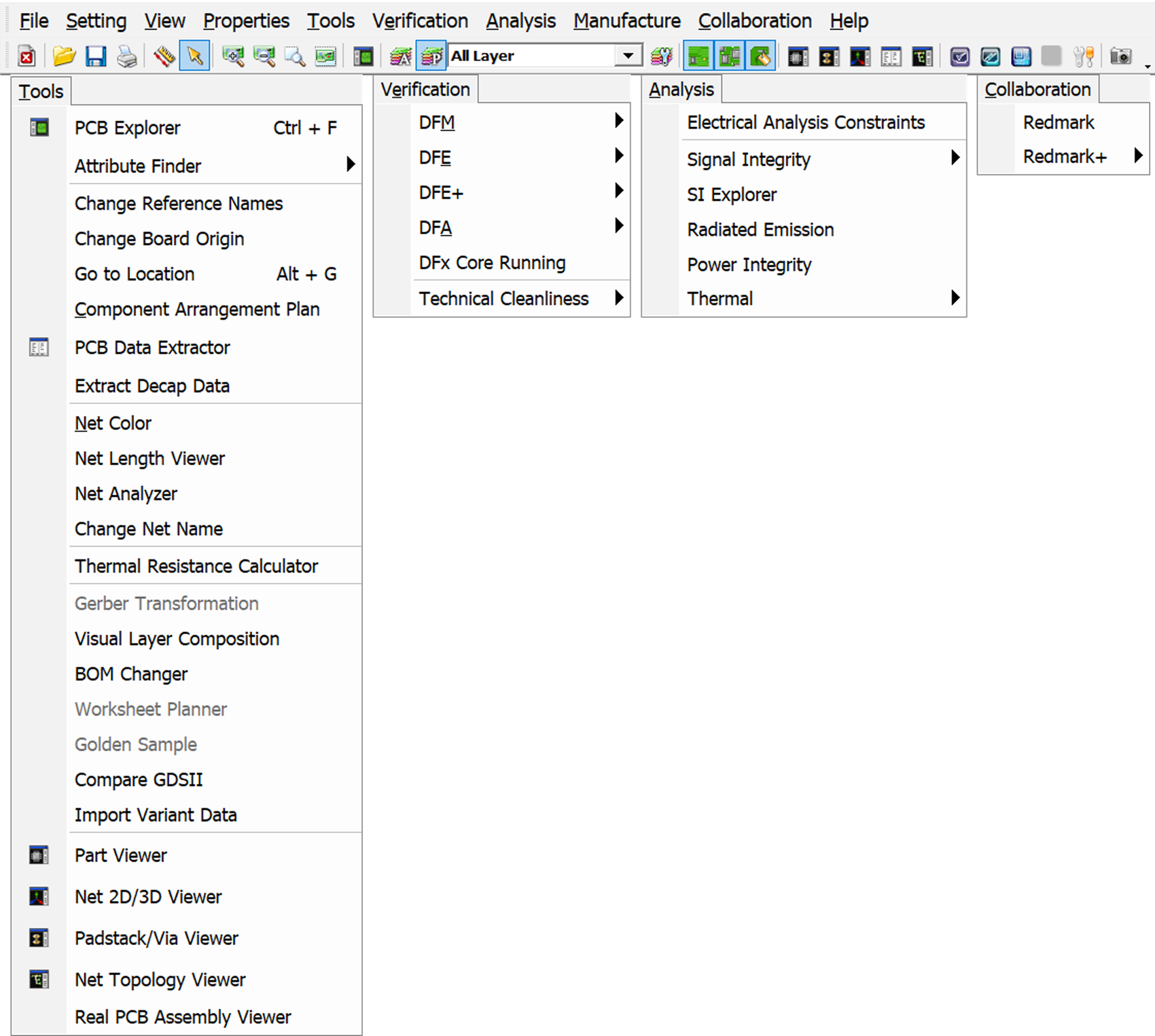
- The Technical Cleanliness feature has been enhanced to export analysis
results to ODB++ format.
Figure 2. Technical Cleanliness result export to ODB++ 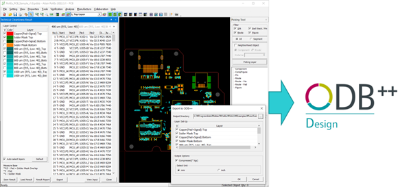
- The Board category in DFM now has a new Layer Stack-up checking
item.
Figure 3. New Layer Stack-up checking item in DFM 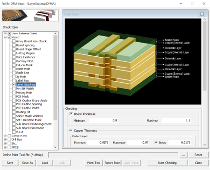
- The Pattern category in DFM now has a new Acute Angle checking
item.
Figure 4. The new Acute Angle checking item in DFM 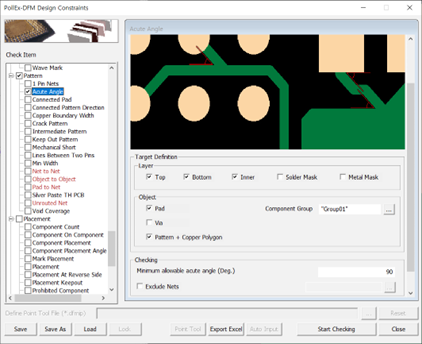
- A new SerDes simulation feature has now been added to Network Analysis for
single or differential lines. This feature verifies the Bathtub and
Statistical eye diagrams for the IBIS-AMI-based SerDes models in SI. A
SerDes system simulation involves a transmitter (Tx) and a receiver (Rx)
connected by a passive analog channel. You can perform statistical analysis
and time-domain analysis. This function will enable you to quickly and
accurately analyze the SerDes full channel composed of PCB, Connector, and
Cable.
Figure 5. SerDes Analysis 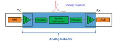
Figure 6. Statistical Eye Diagram: Normal 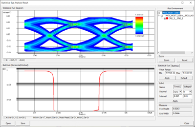
Figure 7. Statistical Eye Diagram: PAM4 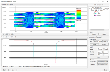
- A new feature to enable automatic setup of pin mapping using Excel has now
been added to the package S-Parameter model in SI. After extracting the
S-Parameter of the package using Network Analysis, you can perform Signal
Integrity Analysis of the entire flow of DIE + Package + PCB more easily by
connecting it to the simulation model. However, to extract the S-Parameter
Model of the Lead Wire of the package, use other 3D tools.
Figure 8. Package S-Parameter extract & insert flow 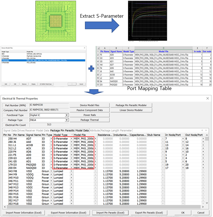
- The IR Drop engine has now been enhanced to mesh 'trace-type net'
which improves accuracy in PI. Since the mesh trace requires more analysis
time, you can select the mesh type and review the Current Density in the
trace-type object based on your requirements.
Figure 9. Mesh-style option 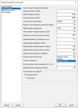
Figure 10. Current Density: Polygon Mesh 
Figure 11. Current Density: Polygon + Trace Mesh 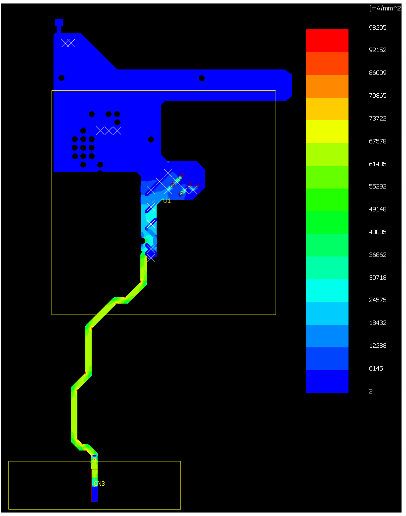
New Features
- PollEx Modeler
- PCB
- The PCB menus have been reorganized to provide better clarity.
- PollEx Verification
- DFM
- Added a new checking item of the Layer Stack-up in the Board category.
- Added a new checking item of the Acute Angle in the Pattern category.
- PollEx Interface from ECAD
- Mentor Graphics Xpedition
- The Siemens Xpedition importer has now been added directly from its binary data using the API.
- PollEx Analysis
- SI
- The SerDes simulation in the Network Analysis, specifically for single lines or differential lines has now been added. It verifies the Bathtub and Statistical eye diagrams for the IBIS-AMI-based SerDes models.
- The Network Parameter of the selected VIAs in the Net Topology Analyzer is added. This enables to extract S/Y/Z parameters, impedance, and equivalent RLGC values between VIAs’ in/out ports.
Enhancements
- PollEx Modeler
- PCB
- The layer setting of the Visual Layer Composition has now been enhanced.
- You can now work on multiple designs without closing opened designed data.
- Modified to display silk on/off in the Real PCB Assembly Viewer.
- PollEx Verification
- DFM
- An option in the BGA item is added to prohibit PTH vias between BGA pads.
- An option to check a number of connected patterns is added to the BGA pad in the BGA item.
- An option is added in the BGA item to check if all patterns connected to the BGA pads have the same thickness.
- Added an option in the Component Spacing 2 item to check the maximum distance between Solder Mask and Pad in the same component.
- Added an option to check if patterns connected to pads with length-width asymmetry are connected through the shorter side in the Connected Pattern Direction item.
- Added an option to check the Tie leg width and length in the Copper Connected Pad item.
- Added an option to check the clearance between the coverlay open area and copper in the Coverlay item.
- Added an option in the Crack Pattern item on whether teardrops are designed on the target component’s pads
- Added an option in the Cutting Region item to recognize only the patterns crossing the PCB outline as JTAG patterns.
- Added an option to check missing pads on all layers of DIP-type holes in the Dip Annular Ring item.
- Added an option to check the existence of S/R covered copper between the Pad edge and exposed pad for specified components like QFN, SON, and DFN in the Edge Pin Size item.
- Added an option in the Hole Distance item to check the clearance between holes and components.
- Added an option to check whether the via hole is located on the component pad's central axis (long axis) in the Hole Through Pad item.
- Added a new check item for the PCB board thickness in the Layer Spec item.
- Added a measure base type of COC+Pad/Solder Mask Overlap in the PCB Outline Spacing item.
- Added an option in the PCB Outline Spacing item to check the clearance for the figure objects.
- Added an option in the Ref Name Silk item to check the clearance between components and reference names.
- Added an option to check the existence of a solder mask between the thermal pad and I/O pad in the Solder Resist Pad item.
- Added an option in the Solder Resist Pad item to check the maximum distance between Solder Mask and Pad in the same component.
- An option to recognize as different nets if other nets are connected to the same reference has been added in the Solder Resist Pad item.
- An option to check the teardrop length has been added in the Teardrop item.
- A BGA measure base in the Underfill item has been added.
- Added an option to verify the maximum number of layers of Laser/Buried/Blind vias that can penetrate in the Via Overstack item.
- An option in the Underfill item has been added to check the clearance between BGA and Via/NPTH/Test Point.
- Enhanced the Link to ECAD feature with the Xpedition to navigate the correct layer.
- PollEx Analysis
- SI
- A new feature to enable automatic setup of pin mapping using Excel has been enhanced to the package S-Parameter model in SI.
- Generated Multiple Models in the Transmission Line Analysis has been enhanced to generate differential line models automatically.
- Enhanced to analyze multiple nets in the Net Topology Analyzer of the Network Analysis. Please note that the coupling effect should be analyzed with the Crosstalk analysis.
- PollEx Interface from ECAD
- Cadence Allegro
- Enhanced the zoom factor when crossprobing with DFx results in the Link to ECAD feature.
Resolved Issues
- The missing build-up VIA pads in the Cadence Allegro importer issue has been fixed.
- A bug in the silk screen text location on the Cadence Allegro importer has been fixed.
- Fixed parse error in the CADVANCE importer.
- The missing particular Artwork layers in the Mentor Board Station importer issue has been fixed.
- The misplaced component pads in the ODB++ importer issue has been fixed.
- Fixed a bug with incorrect arc direction in the DXF exporter.
- The Auto Naming option on the DFx Core Running bug has been fixed.
- Incorrect grouping of Sub-Items in the Result Table of Copper Cross Over Item in DFE issue has been fixed. The same option was displayed in duplicate in several Sub-Items.
- An issue for not recognizing holes declared as Components in the Power Net to Net item of DFE has been fixed.
- An issue that a single-ended net is displayed in the differential net category when displaying impedance check results in the DFE+ is resolved.
- Fixed an issue to open the Net Topology Analyzer of the Network Analysis in the SI after assigning the Package S-Parameter.
- An issue where Crosstalk Analysis could not be performed when a space was included in the VIA name has been fixed.
- Resolved an issue that the IBIS model existing in the Part Directory is not assigned when executing the Properties/Part menu.
- An issue that analysis is not possible when the passive component is directly connected to the plane without trace during the IR-Drop Analysis has been solved.