Power Rail Group Type Setup
To perform a Stress Test, the voltage value of each power and ground nets should be defined.
You can define voltage values of each power net and voltage of voltage divide logic.
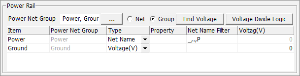
Figure 1.
- Power Net Group: Select power and ground net group to define voltage value.
- Net: Upon selecting this menu, all the selected power and ground nets are listed in the table below.
- Group: Upon selecting this menu, all the selected power and ground groups are listed in the table below.
- Find Voltage: Upon clicking this button, the voltage value of power and ground nets are displayed in the table below. To execute this menu, the table below must be setup first.
There are three types: Pin Property, Net Name, and Voltage types.
- Pin Property: You can assign power value using pin property of component which is connected to each power net.
- Net Name: If the power net name contains a voltage value information, you can assign power value using net name string of power net.
- Voltage(V): You can enter voltage value of power net.
Power Rail Group Setup
-
Select a Type and follow the steps for each:
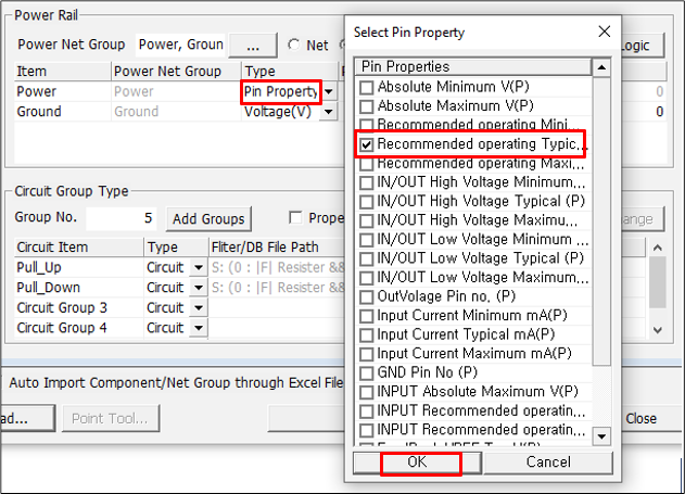
Figure 2.- To assign power
value using pin property of component which is connected to each power
net, select Pin Property.
- Click the empty Property field to open the Select Pin Property dialog.
- Select the appropriate property, and then click OK.
- To assign power
value using net name string of power net, select Net
Name
- Enter the
voltage separator in the Net Name Filter field.Note: The voltage separator means that the character used to distinguish the decimal point of voltage. Ex: VCC1P8 => the voltage separator is P Ex: VCC1.8 => the voltage separator is “.” In this case, enter “.,P” as a voltage separator.
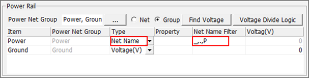
Figure 3.
- Enter the
voltage separator in the Net Name Filter field.
- To enter your own
voltage value, select Voltage(V).
- Enter the voltage value directly in the Voltage(V) filed.
- To assign power
value using pin property of component which is connected to each power
net, select Pin Property.
-
Find Voltage: Upon clicking this button, the voltage
value of power and ground nets are displayed in the table below.
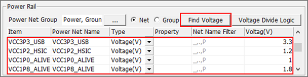
Figure 4.
Voltage Divide Logic
You can find out the exact voltage value of voltage divide logic.
-
Voltage Divide Component Section: In this step, we set up the component list
used for voltage divide logic and property in which the resistance value is
declared.
-
Component: Select component group used for voltage divide logic.
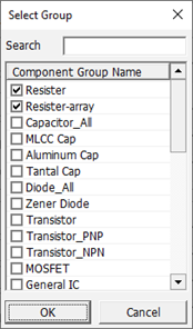
Figure 5. -
Component Value: Select property in which the resistance value is
declared.
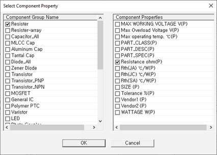
Figure 6.
-
Component: Select component group used for voltage divide logic.
-
Short Pin Section: TR or FET is a device with three pins, so it needs
information about pins connected to each other during short processing.
-
Short Pin-By Pin Name: Declare pin paring information as pin name. If
there is more than one condition, the separator “,” is used.
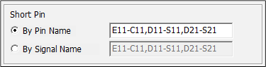
Figure 7. -
Short Pin-By Signal Name: Declare pin paring information as signal
name. If there is more than one condition, the separator “,” is
used.
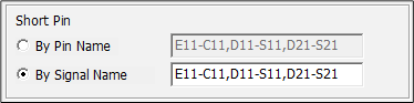
Figure 8.
-
Short Pin-By Pin Name: Declare pin paring information as pin name. If
there is more than one condition, the separator “,” is used.
-
Consider Turn-on Voltage-Base Power Section: In this step, we declare the base
power net to start navigation, and declare the power component used for power
logic.
-
Consider Turn-on Voltage: Upon selecting this option, consider turn-on
voltage during power navigation.
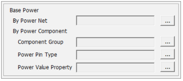
-
By Power Component: Declare base power net to start navigation using
component. Among the power nets, power nets that connected to specific
pin of specific component are selected as base power net.
- Component Group: Select Component Group. Normally, the primary power comes from a power component such as DCDC converter.
- Power Pin Type: Select Power Pin Type. Among the power nets,
power nets that connected to this type of pin are selected as
base power net.
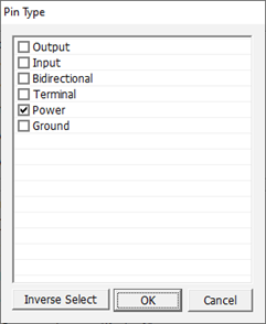
Figure 9. - Power Value Property: Select property in which the power value
is declared.
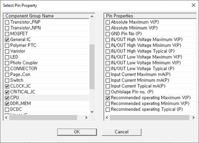
Figure 10.
-
Consider Turn-on Voltage: Upon selecting this option, consider turn-on
voltage during power navigation.
-
Consider Turn-on Voltage-Component Section:
-
Turn-on Voltage Section: In this step, we declare the turn-voltage of each
component group to be used during power navigation.
-
Voltage(V): Enter turn-voltage directly or select property in which the
turn-on voltage is declared.
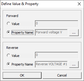
Figure 11.
-
Voltage(V): Enter turn-voltage directly or select property in which the
turn-on voltage is declared.
-
Show Voltage Divide Data & Voltage Assigned Data Section: In this step, you
can review the voltage of voltage divide logic.
-
Show Voltage Divide Data & Voltage Assigned Data: Upon clicking
this button, the voltage of each voltage divide logic will be
displayed.
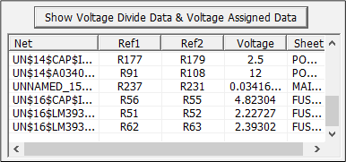
Figure 12.
-
Show Voltage Divide Data & Voltage Assigned Data: Upon clicking
this button, the voltage of each voltage divide logic will be
displayed.