
Category: Toolbox > eDrives > Inverters
Inputs:
•VSA: Input DC bus voltage of the first two phases.
•VSB: Input DC bus voltage of the third phase.
•EN[1..3]: Vector input enabling each phase (half-bridge) of the three-phase gate logic. (Phase leg x switches are enabled when EN[x] ≥ 1.)
•IN[1..3]: Vector input controlling each phase of the three-phase gate logic. (High-side switch x is ON and low-side switch x is OFF when IN[x] ≥ 1.)
•CP[+,-]: Comparator positive and negative inputs.
•DIAG/EN(in): Input enable pin of all three phases.
•lout[1,2,3]: Three-phase output current (A) fed back into the model.
•Vload[1,2,3]: Three-phase output (load) voltage fed back into the model. (optional)
Outputs:
•OutNt[1,2,3]: Three-phase line-to-neutral output voltage.
•OutLL[12,23,31]: Three-phase line-to-line output voltage.
•Vboot: Boot-strap voltage.
•VCP Charge-pump voltage. (ideal)
•CPout: Comparator output.
•DIAG/EN(out): Set low (zero) if an over-current is detected.
•lin: DC input current (A) of the device.
•vlsense[1,2,3]: Three-phase current sense outputs normally fed into current sense resistors. In this case, the current sense resistors are included in the model and the three-phase output is the voltages dropped across the internal current sense resistors.
Description: The L6230 Inverter block is a switching model of a three-phase inverter bridge. It specifically models the L6230 chip from ST (https://www.st.com/en/motor-drivers/l6230.html).
The input and output pins of this model mirror the input and output pins of the L6230:
Source: ST L6230 datasheet DocID18094 Rev 3. https://www.st.com/resource/en/datasheet/l6230.pdf
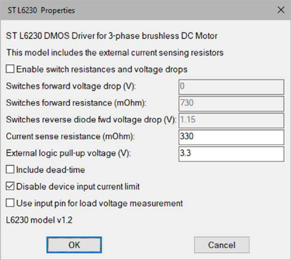
Current sense resistance (mOhm): Indicates the resistance value of the three-phase current sensing resistors. The output at v_Isense will then be Iout*Rsense for each of the three phases. Note that the sense resistors are included in the model.
Disable device input current limit: Disables the L6230 input (supply) current limit threshold of 2.8A typical.
Enable switch resistances and voltage drops: Enables the inclusion of the internal switches resistance and the switches voltage drop.
External logic pull-up voltage (V): Determines the output value at the VCPout and DIAG/ENout pins, assuming an internal pull-up.
Include dead-time: Enables the L6230 fixed dead-time of 1us.
Switches forward resistance (mOhm): Indicates the forward resistance of the half-bridge MOSFETs. The typical ON-resistance of the L6230 at 25 °C is 730 mOhm.
Switches forward voltage drop (V): Since the half-bridge switches are MOSFETs in the L6230, this value is typically 0 V.
Switches reverse diode fwd voltage drop (V): Indicates the forward voltage of the integrated MOSFET reverse diodes. This value is typically 1.15 V at 1.4A output current for the L6230.
Use input pin for load voltage measurement: The load voltage measurement can be used to correctly represent the output phase voltages when both half-bridge switches are off (during the dead-time). If this parameter is not activated, the load voltage will be estimated during the dead-time transition assuming a balanced three-phase load.